Lab 5 -
EE 421L
Authored
by Min Lan,
LANM2@UNLV.NEVADA.EDU
10/04/2013
Electric library: ML_ee421L_f13_lab5.jelib
Lab
description
In this lab, we will create two inverters (one is 20/10, the other is 100/50)
and simulate them with SPICE, ALS, and IRSIM.
Schematics
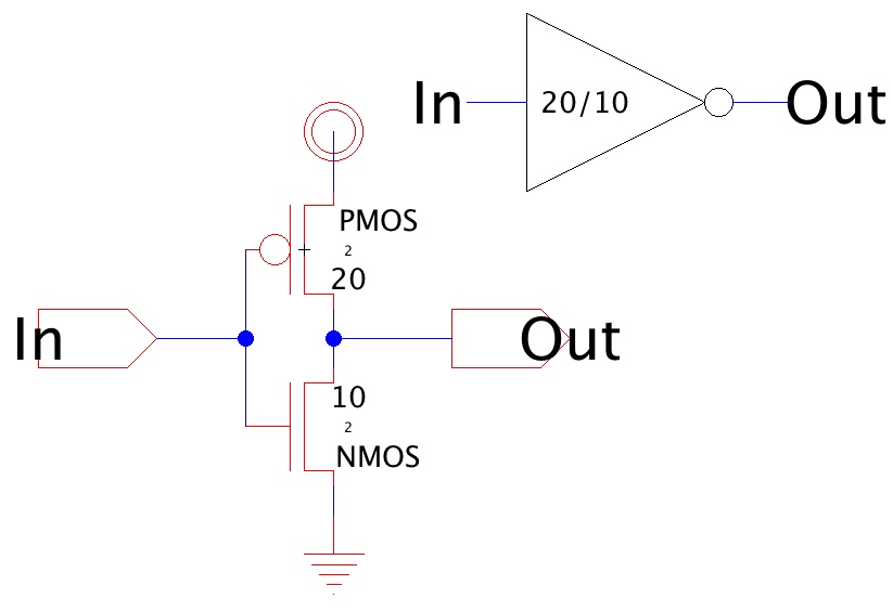
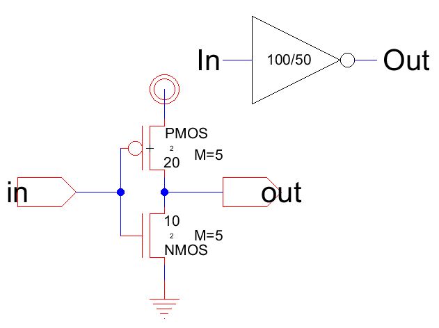
- Create a new cell for the 20/10 inverter, named <your_initials>_inv_20_10
- From the Lab 4, copy the NMOS_IV and PMOS_IV cells to the library for this lab.

- Go the schematics cell of NMOS_IV, select the NMOS node and press Ctrl + C to copy
- Then paste it in to the new inv_20_10 cell.
- Repeat for PMOS_IV
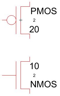
- Change the width of PMOS to 20 and width of NMOS to 10, and make sure the length
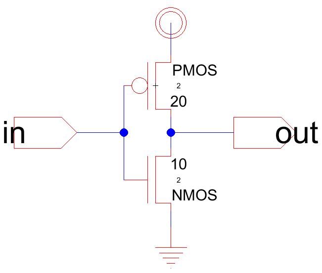
is at least 2 (No changes from Lab 4 in this case). - Place the PMOS above the NMOS, connect the their gates with an arc and connect
the Drain terminals of the MOSFETs with an arc. - Add power node and ground node to the cell, change the sizes of the nodes to match
other elements in the cell, connect power to the S of PMOS and ground to S of NMOS. - Also add two off-page connectors and export them for in and out voltages.
- Connect export "in" to the gates, and "out" to the drains.
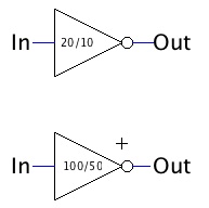
Icon
- From the View menu, select Make Icon View
- Go to the generated inv_20_10{ic} cell, delete everything except the arcs and exports.
- Select the "out" export and its connected arc, rotate them until the text is on the right

- Place a triangle on the icon cell, rotate the isoceles triangle so that the legs are
symmetric to the horizontal axis. - Move the "in" export so that it touches the base of the triangle from the left.
- Move the "out" export towards the tip of the triangle, leave one grid space for the
bubble.
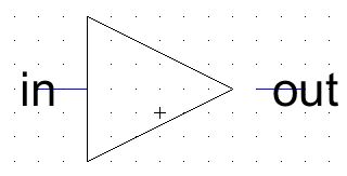
- Place a circle on the cell, change the x and y sizes to 1, finally move the circle to
the reserved grid space.
- Turn off the grid (Ctrl-G), go up (Ctrl-U) to schematic, and we have:

For 100/50 inverter
- For the second inverter, simply duplicate the first cell group, and rename the copy
<your_initials>_inv_100_50 - We will implement this inverter with multiplier, ie. place 5 MOSFETs in parallel
- To set the multiplier, select the PMOS node, and go to menu Tools >> Simulation
(Spice) >> Add Multiplier - A new text will appear on the cell, Change M=1 to M=5 for this lab (100/20 = 5)
- Repeat for the NMOS node.
Layout
20/10 inverter
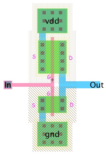
- Create a cell for layout, you can create it by select menu View >> Edit Layout View,
you will then be asked if you want to create one if it is not created yet. - Place the components on the layout cell
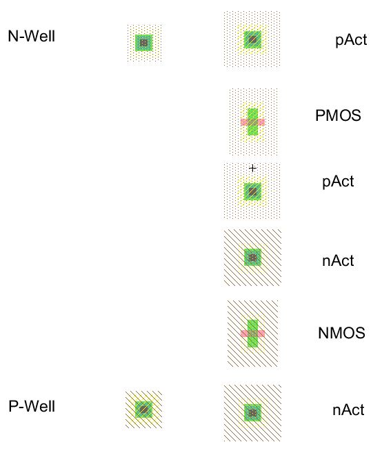
- Make change the size of the elements:
- PMOS, pAct : set x size to 20
- NMOS, nAct: set x size to 10
- N-Well, P-Well: set x and y sizes to 18 by 15
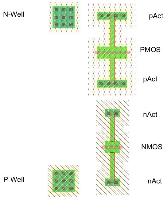
Note: set the End Extension of the active arcs to "Neither End" to avoid error
DRC'ing- Move the Actives towards their respective MOSFET
- Selects the MOSFETs and rotate them 90 degrees (cw or ccw)

Note the terminals of the MOSFETs:
- PMOS: Source on the left, Drain on the right
- NMOS: Drain on the left, Source on the right
- Place the N-Well above the PMOS with their dots overlapped, and place the
P-Well below the NMOS with their shades overlapped.
- Export the square N-Well contact to vdd and export the P-Well contatct to
gnd
- Place an Metal-1-Poly-1-Contact and an Metal-1-Pin for In and Out exports.
- Connect the MOSFETs together accordingly to match the schematics


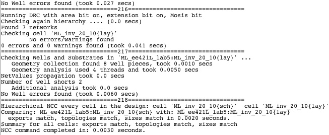
- Check your layout against DRC, NCC, and ERC

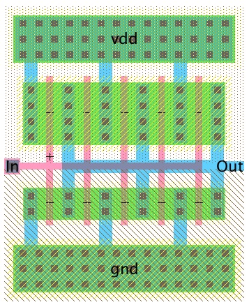
100/50 inverter
- Duplicate the 20/10 inverter's layout and name it <your initials>_inv_100_50
- Make 4 additional copies of each MOSFET and place them to the right of
the original. Separate the MOSFET so that there is enough space to place
an Metal-1-Active-Contact between two adjacent MOSFETs.
- Make copies of the Metal-1-Active-Contact and place one to the right of
every MOSFETs.
- Change the x sizes of the N-Well and P-Well pins to 70 for the larger layout
- Move the Out export far right to reflect the layout changes

- Connect the MOSFETs to adjacent Active Pins
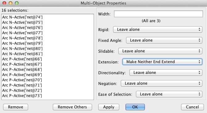
- Select all the Active arcs and press Ctrl-I, int the Multi-Object Properties
window, change the Extension to "Make Neither End Extend"

Now the arcs will not extend beyond the thin "plates" of the MOSFETs
Move the MOSFETs and Active-Pin togethers until they overlap.
- Start with the leftmost P-Active Pin, connect the Pin to the vdd, connect the
next the N-Active-Pin below it, and connect next Pin to vdd and so on.
- Connect non-connected N-Active-Pins to the gnd, and connect gates together

- Check your layout against DRC, ERC, NCC

Simulation
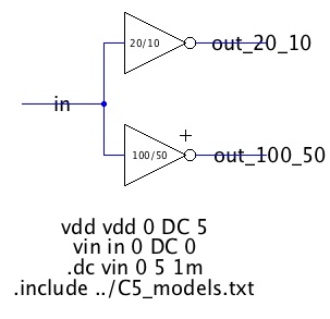
We will be simulating both inverters in the same schematic for each
type of simulation.
SPICE:
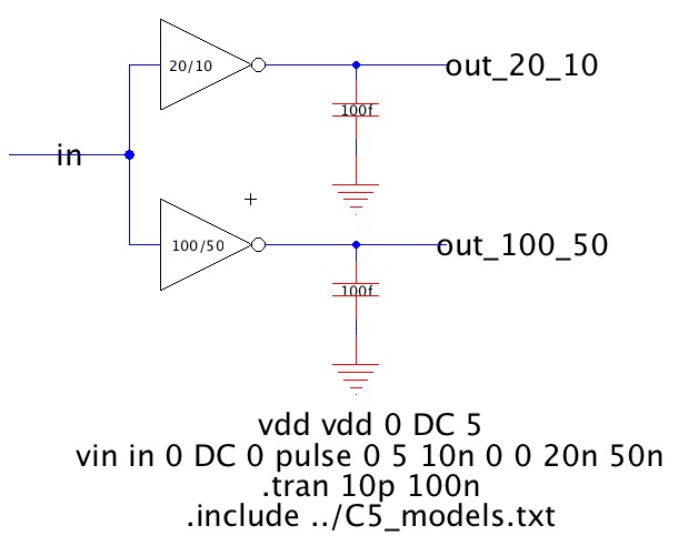
- Create a new cell called <your_initials>_sim_inv_SPICE
- Drag the inverters' icons into the cell.

- Connect input of the inverters together, and draw an arc to the left.
Draw an arc from the output of each inverter, name the nodes
out_20_10 and out_100_50 respectively.
- Add spice code to simulate the inverters without load

- DRC and simulate

- To simulate the delay with load, place the load capacitor under each output
- Change the spice code to do a transient analysis with an pulse input

The schematics for different loads are the same except for the capacitor
value. To create the schematics for different loads, right click the
schematic in the explorer, select "Create New Version of Cell". Unfold the
group and rename the cell under the group. When asked to rename the
previous versions of cell, click No. Make the changes needed, and repeat
for different loads.
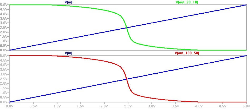
- Simulation Results
- 20/10 inverters (Top to bottom: 100fF, 1pF, 10pF)


The increasing capacitance increase the rise-time and fall-time, in the 3rd image,
the delay is too long for high frequency switching.
- 100/50 inverters (top to bottom: 100fF, 1pF, 10pF)


Using a larger inverter, the capacitors' effect in switching delay is less
significant. The larger inverter is able to drive a larger load.
ALS:
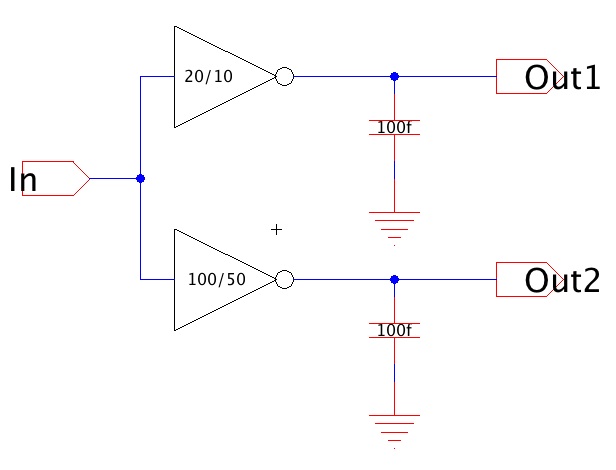
- Different from the SPICE simulation, the ALS uses Exports with off-page
connectors

- From menu Tool >> Simulation (Built-in), select "ALS: Simulate Current Cell".
In the simulation window, delete unnecessary signals and leave only IN_,
OUT1, OUT2.
- Select the IN_ signal, go to menu Tool >> Simulation (Built-in), select
"Set Clock on Selected Signal...". The input and output reflect changes.
- Top to bottom (100fF, 1pF, 10pF)


- There seem to be no difference in delays for differenct loads.
Conclusion: ALS is only for functional analysis.
IRSIM:
- Similar to the ALS, but create a new schematic for each inverter
- Go to menu Tools >> Simulation (Built-in), select
"IRSIM: Simulate Current Cell"
- Save your stimuli by going to menu Tools >> Simulation (Built-in),
select "Save Stimuli to Disk", you can several simulation without
redrawing
- (for each capacitance, top is 20/10 inverter, bottom is 100/50)
- The IRSIM can show the delays for different capacitive loads.
Backup
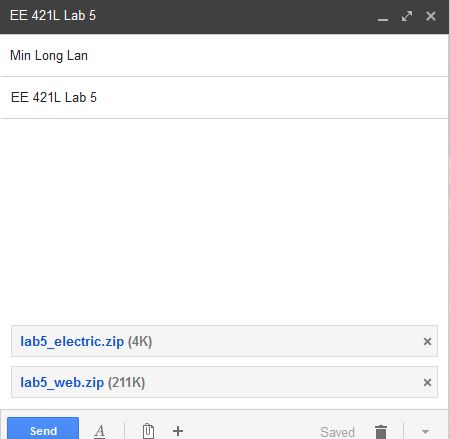
Zip both your library file and your webpages and email to yourself.
Return to EE 421L Labs
