Lab 4 -
EE 421L
Authored
by Min Lan,
LANM2@UNLV.NEVADA.EDU
09/27/2013
Electric Library: ML_ee421L_f13_lab4.jelib
SPICE models: C5_models.txt
Lab
description
In this lab, we will be drawing the schematics and laying out NMOS and PMOS.
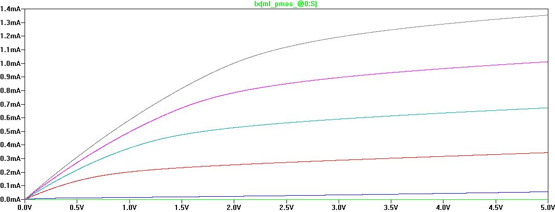
We will also simulate the I-V characteristics of the MOSFETs.
Schematics
- Create a schematic cell for NMOS and PMOS, named
<your initials>_NMOS_IV
and <your_initials>_PMOS_IV respectively.
- Set the width of the NMOS to 10, and the width of PMOS to
20. Leave the length as 2.
- From menu >> Tools >>
Simulation (spice), select Set Spice Model..., and change the text to
NMOS
- Move the texts (and rotate and needed) as appear below
- For PMOS, especially for a 4-terminal one, we want the
source terminal to be on the top and
the drain terminal on the bottom, so go to menu Edit >>
Mirror >>, select Up < - > Down
- For a 3-terminal MOSFET, the D and S terminal appear the
same, selecting the terminal tells
which is which.

- Use 3 off-page connectors to connect the 3 terminals,
create exports for the off-page connectors

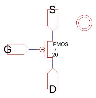
- Note that a GND node is placed on the schematics of NMOS to
match the gnd export that we
will be included in the layout, similarly a power node is placed on
PMOS_IV{sch}.
- To simulate the schematics, create a new cell for both NMOS
and PMOS, prefixed sim_
- Drag the schematic from the explorer into the new created
cell, select the blank box
click on the One Level Down button to reveal the inner parts

- Draw an arc from the exports G and D, label them G, D.
- For NMOS, connect S terminal to gnd; for PMOS, connect S
terminal to vdd.
- Press F5 to DRC the schematics
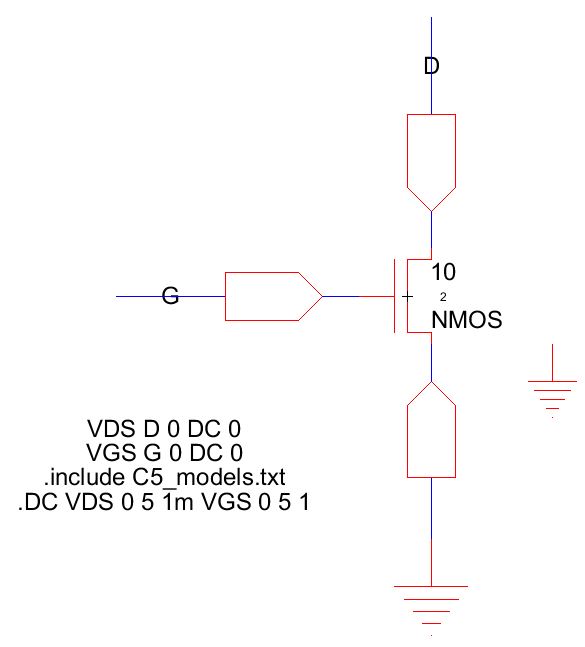
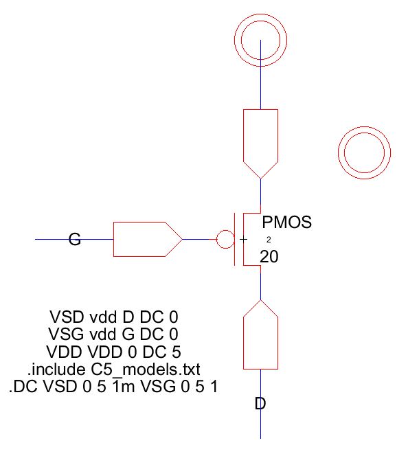
- Add spice codes to simulate the circuit
- sim_NMOS_IV
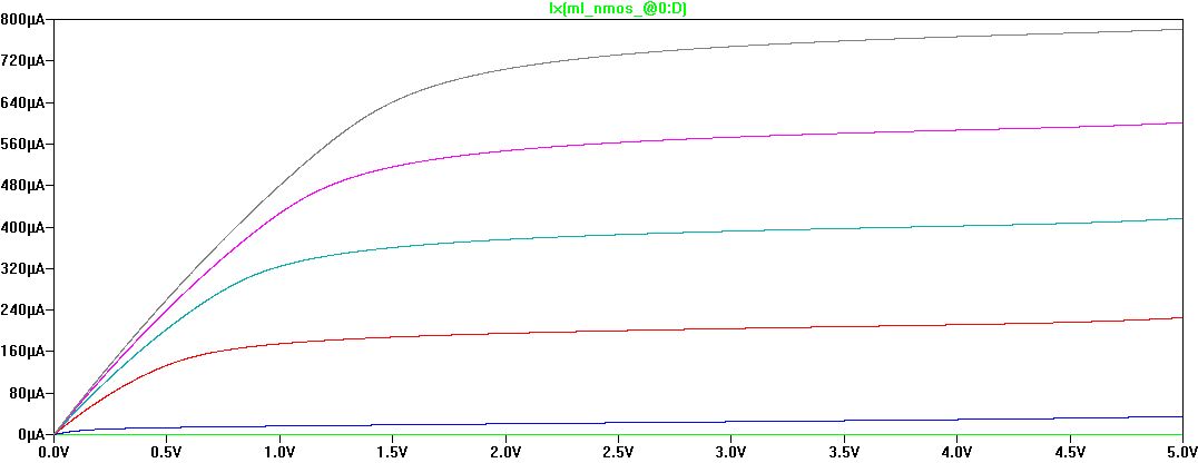
- sim_PMOS_IV
Layout
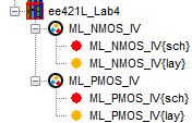
- Create a layout cell for both NMOS and PMOS with
the same name, they will be automatically
grouped
- Place components on the cell window
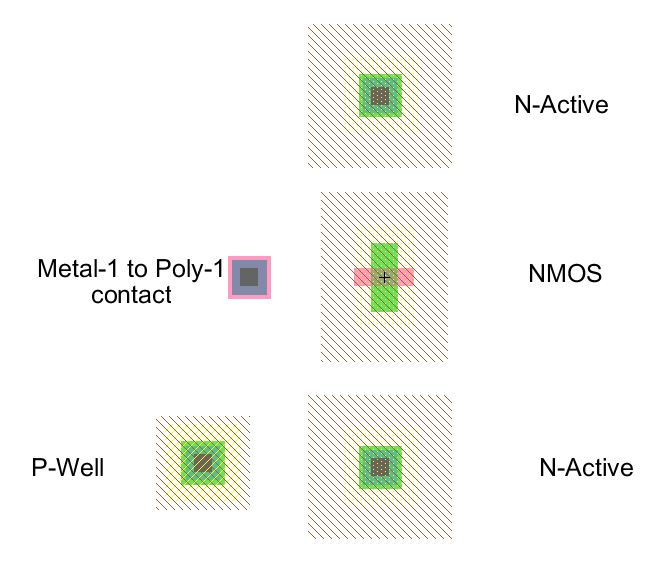
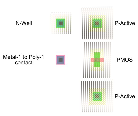
- Set the X-size of the MOSFETs and the Actives to their corresponding width
(10 for NMOS, 20 for PMOS) - Set the the X-size of the P-Well node (NMOS) and the N-Well node (PMOS) to 10.
- NMOS
- Connect the drain terminal to the upper N-Active node and the source terminal to the
lower N-Active node
- PMOS
- Connect the source terminal to the upper P-Active node and the drain terminal to the
lower P-Active node
- For both MOSFETs, select the pink poly, Set Spice Model via menu Tools >> Simulation (Spice)
- Change the texts to NMOS and PMOS respectively
- Move the Actives towards the MOSFET until they overlap, also move the P-Well in NMOS
(N-Well for PMOS) so the it overlaps with the substrate. - Connect the Metal-1-Poly-1-Contact to the Poly-1 of the MOSFETs
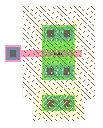
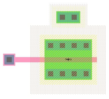
- Draw a Metal arc from the 4 contacts; create exports at the metal nodes
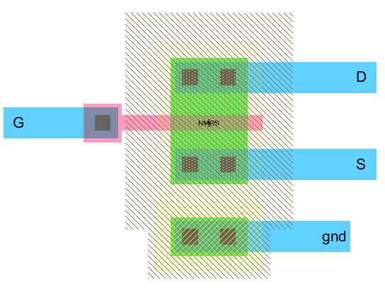

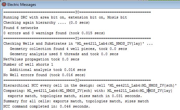
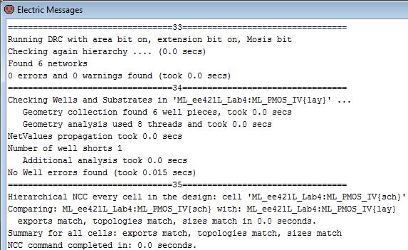
- Do DRC, ERC (Well Check), NCC checks
- NMOS
- PMOS
Backup
Zip both your library file and your webpages and email to yourself.

Return to EE 421L Labs