Lab 3 - EE
421L
Authored
by Min Lan,
LANM2@UNLV.NEVADA.EDU
09/21/2013
Note: Click on images for original size in a new window/tab.
Electric Library: ML_ee421L_f13_lab3.jelib
Lab
description
In this we will layout the 10-bit DAC designed in Lab 2, also we will
create
icons
of components for use in the schematics.
Review
for R2R DAC:
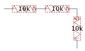
The 10-bit R2R is composed of cascading groups of resistors connected in
L
shape.


Schematics
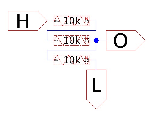
and Icon of R2R group
- Place all 3 resistors horizontally and stack them from bottom up.
- Wire the left pin of a resistor to the right pin of the resistor
above it
- Create exports for the group:
- Top left (Named H) ->
connect to the switch of Bit i
- Middle right (Named O) -> connect to the group above
- Bottom right (Named L) -> connect to the group below
- Create icon from menu View >> Make Icon View
- Choose the generated icon, press Control-D to edit icon
- Delete everything except for exports and draw icon with
Opened-Thicker-Polygon
- DRC the schematics


Edit
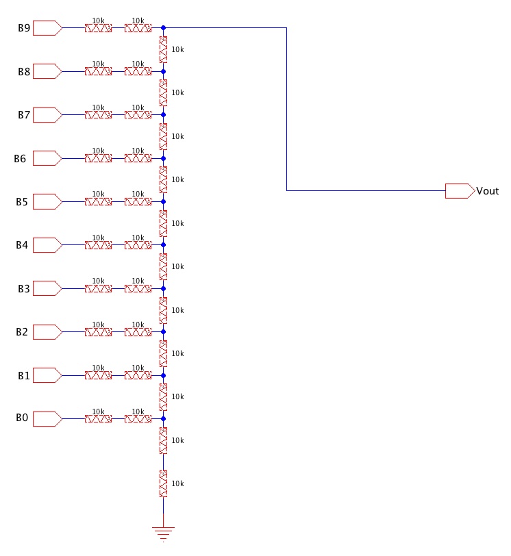
DAC Schematics
- Replace the resistors
with the L shaped icon by dragging the icon
from the explorer into the schematics window.
- Do not forget that
there is one more 10k resistor at the bottom,
use a single N-well resistor for that.
- Press F5 to DRC the circuit
- If found extra pins, press F4 to clean up those pins.

 (DAC_R2R_sch)
Simulation

Layout
N-Well Resistor
Selecting the width and length of a resistor:
The resistor to be laid out is 10kΩ.
Our process has sheet resistance of 800Ω per square.
(More info in the PROCESS PARAMETERS section, look
for N_W column.)
Squares needed = 10kΩ / 800Ω = 12.5 squares.
I selected the width to be 15, therefore the length will be 15*12.5 =
187.5
These values are the same as that used in Lab 2, no change is made in
the
schematics.


How Electric measure the resistor's width and length:
Because of natural of the corner, the resistance near the contact are lower.
Eletric measures the length starting after the contact to where it
meets the other contact.
From the above layout, the width and length of the resistor are the width
of the red rectangle.
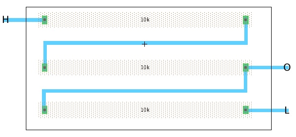
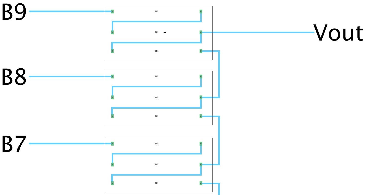
Layout a group of 3 resistor
- As with the schematics
the resistors will be laid "flat".
- Follow similar steps in
the schematics to connect the resistors with
Metal 1
- Create the same set of
exports as the schematics, you have to select
a Metal 1 node before you can create the export

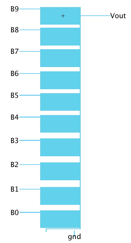
Layout of DAC
- Similar to the
schematics, 10 groups of resistors are stacked bottom up
- For each box counted
from the top, connect using Metal 1 the L export
to the O export of the box underneath it.

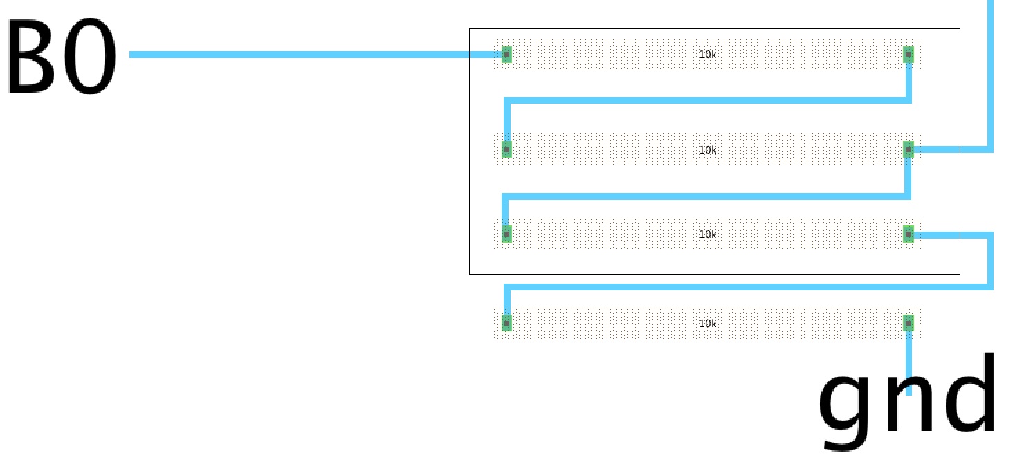
- At the bottom, copy one
10k N-well resistor from R2R layout.
- Connect to lowest L
export to the left pin of the copied resistor.

- Extend Metal 1 of the H
exports of all boxes and create new exports
named B9 to B0 from top to bottom
- Extend the top right O
export and create a new export named Vout
- Also draw a Metal 1
wire from the right pin of the bottom resistor,
create an export and name it "gnd", in lowercase.
Final Layout

DRC, NCC, ERC Checks
DRC: check if layout matches the design rules.

NCC: check if the schematics and layout match each others in exports
topologies, and sizes.

ERC: check wells over user preferences (whether or not N-wells
are connected to vdd, P-wells connected to gnd; the former is
required for digital circuits but is unchecked for this lab)

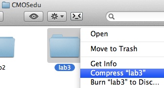
Backup your works!


Return to EE 421 Labs
