check marks and finally hit Done.
After wards you will be able to select from several schematics. Select "sim_ADC_DAC". Note that
you should duplicate this schematic before making any changes.
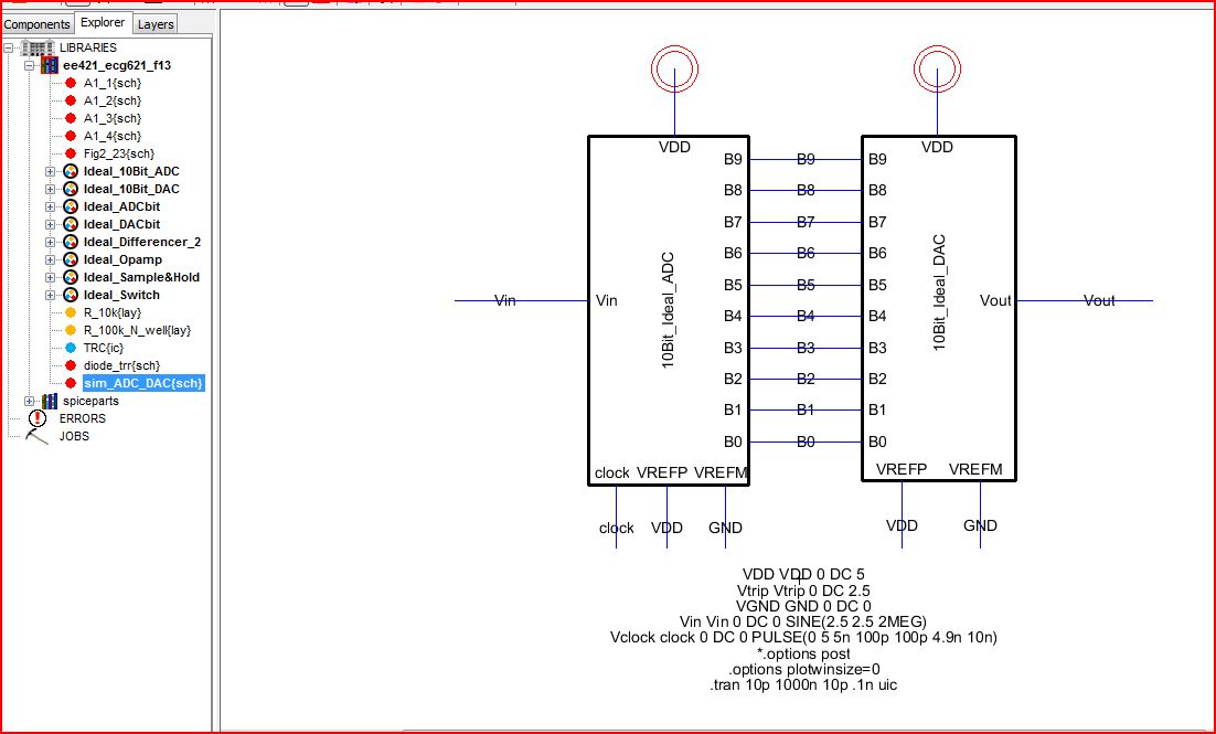
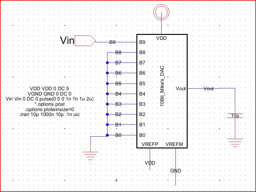
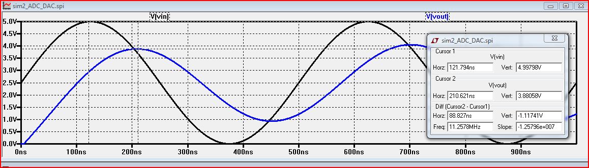
Next, you will simulate the schematic. Be sure to plot Vout & Vin. You should get something like this....
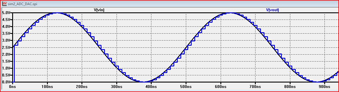
Notice how Vout is similar to Vin except that Vin is not smooth. Vin is the digital signal imitating the analog
sine wave. It is important to know that the small increases of Vin are called the LSB (Least Significant Bit).
It is calculated by taking the VDD and dividing by 2^N (where N is the number of bits). In this case the
we are applying a VDD of 5 volts and we have 10 bits. Therefore our LSB is roughly 5 mV. As you look on the simulation
you can see that that small increases are about 5 mV rises.
Finally, remember to save and backup all of your work!
Postlab:
#1
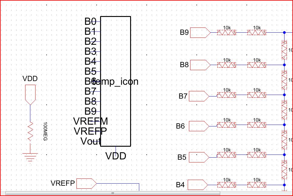
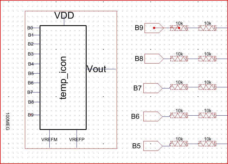
The first thing to do is build your DAC circuit. You will want to use n-well 10k resistors for this.
It would be easier to duplicate "Ideal_10Bit_DAC" from you library. From this selected schematic use
be able to use the DAC icon and build your circuit with it.

You will want to use the circles in blue items along with all of the label tags (B0 - B9)
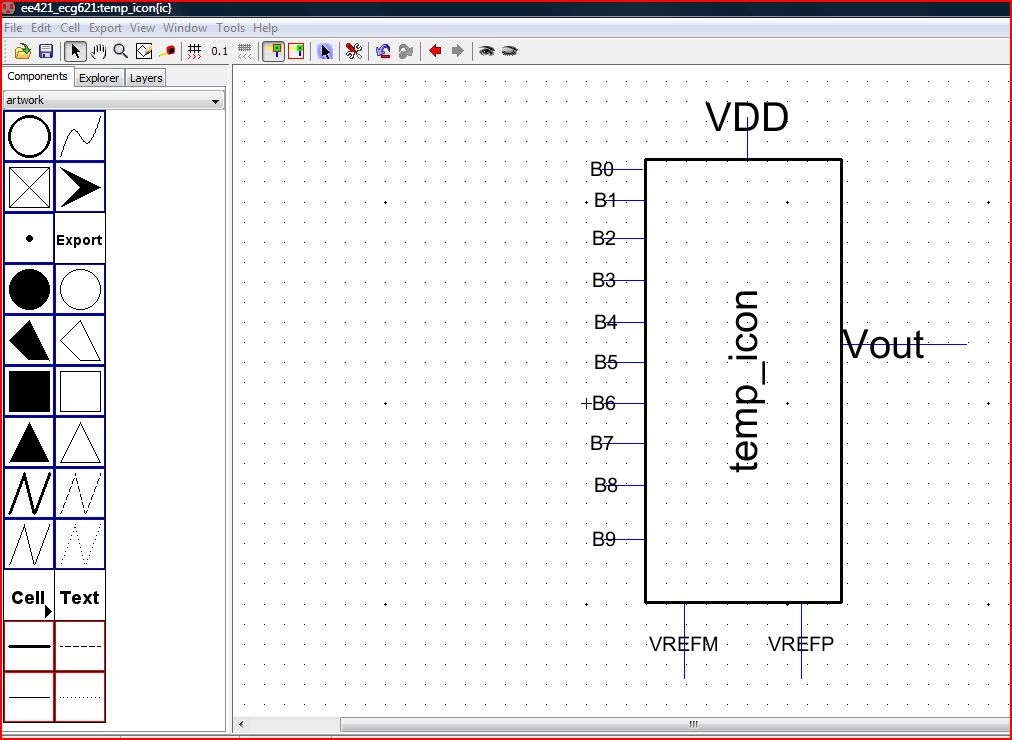
You finished circuit should look like this...
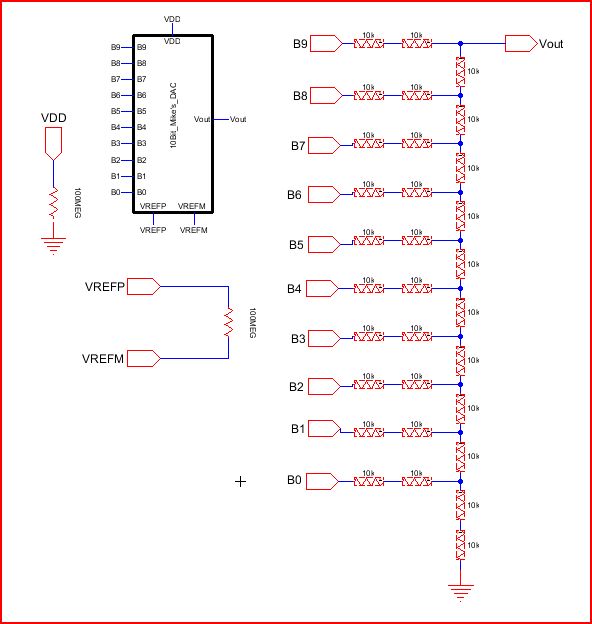
Note that when placing the input/output tabs
you need to label them (B0-B9) using "ctrl E" after clicking on the label/tag. This
will ensure proper routing to the icon.
When you have finished building this circuit you will replace the original DAC , found in the "sim_ADC_DAC",
with the one you just designed. All you have to do is open your duplicate version of "sim_ADC_DAC".
Look at your library list and from the file where you designed your DAC, drag the file below it over into the right. The file from the library will
have a blue circle besides it, indicating that it is an icon. As you drag it you will be able to drop that icon anywhere on the schematic/design
window. Once you made the replacement, be sure all appropriate connects are made, and hit F5 to verify.
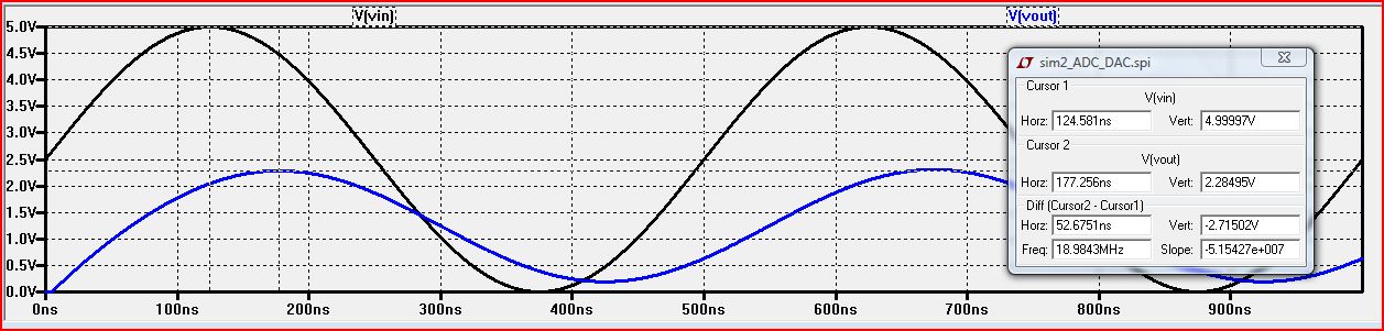
Next run your simulation and compare to your simulation from the prelab.
As you can see the simulation is the same, therefore it was done correctly.
#2
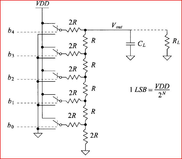
From the schematic you can easily determine the output resistance. Starting from the bottom, or at ground,
Notice that you have two 10k in series & in parallel with two others. These can be written as two 20k's in parallel.
Form circuit theory we know that the resistance will be half, if the two resistors in parallel are equal value.
Therefore the resistance of these two resistors is 10k. This 10k will be added in series with the 10k above it, giving you 20k.
Again, you will have 20k in parallel with 20k. As you move up the schematic, adding the resistors up, you will see that
the total output resistance will be 10k. Also note that if you were to drive a 10k resistive load, you will have an output voltage
that will be half of the input voltage. We know that in a voltage divider, if you were to divide a voltage among two equal valued
resistors in parallel, you will yield half of the input voltage at the output. We will demonstrate this later on.
#3
For this part we will discuss the time delay of the DAC circuit driving a capacitative load.