Lab 1 - ECE 421L
Authored
by Michael Kajkowski,
8/30/2013
1. Setting up Electric
For this lab we will be setting up Electric & learning how to publish our web pages to the CMOSedu site.
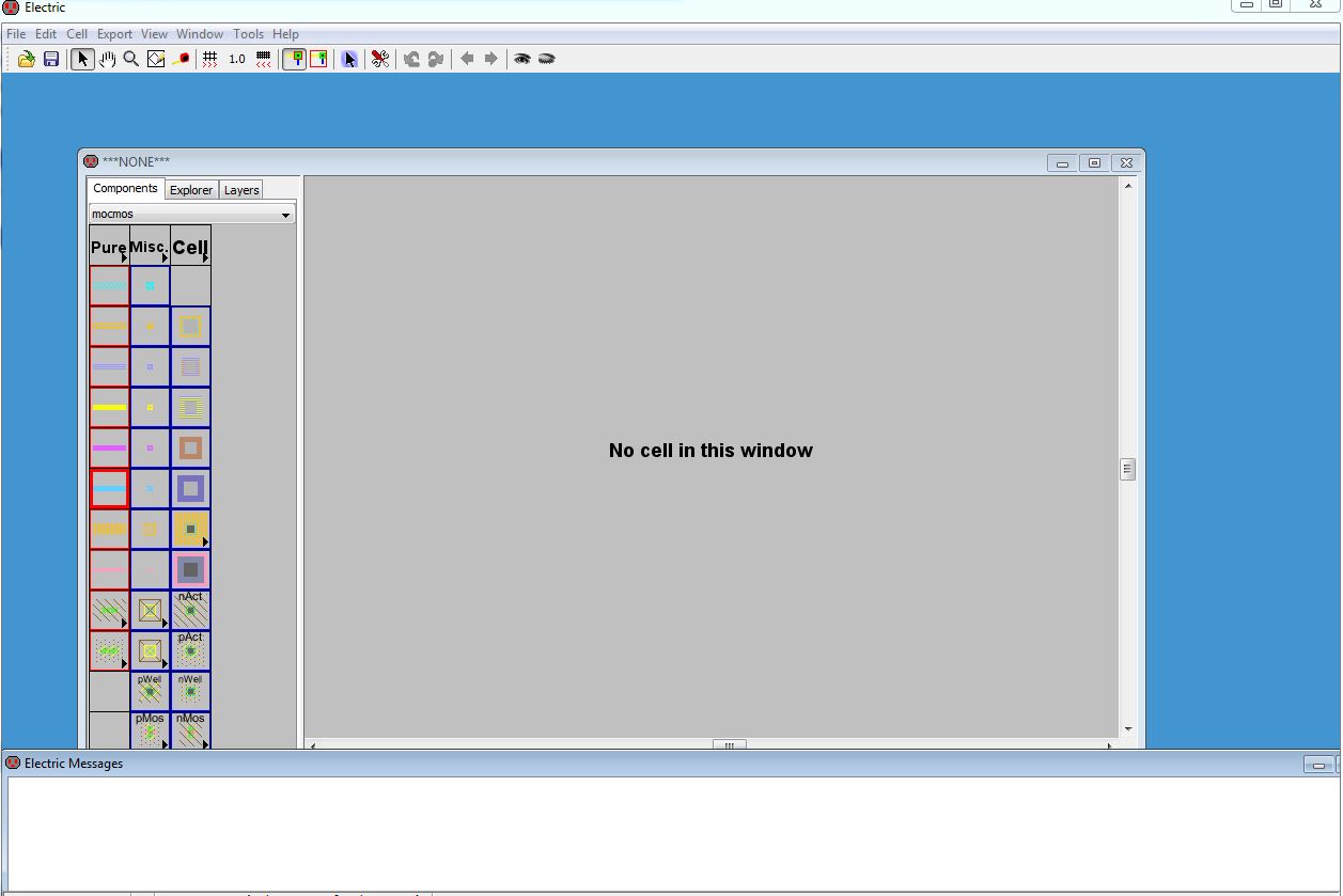
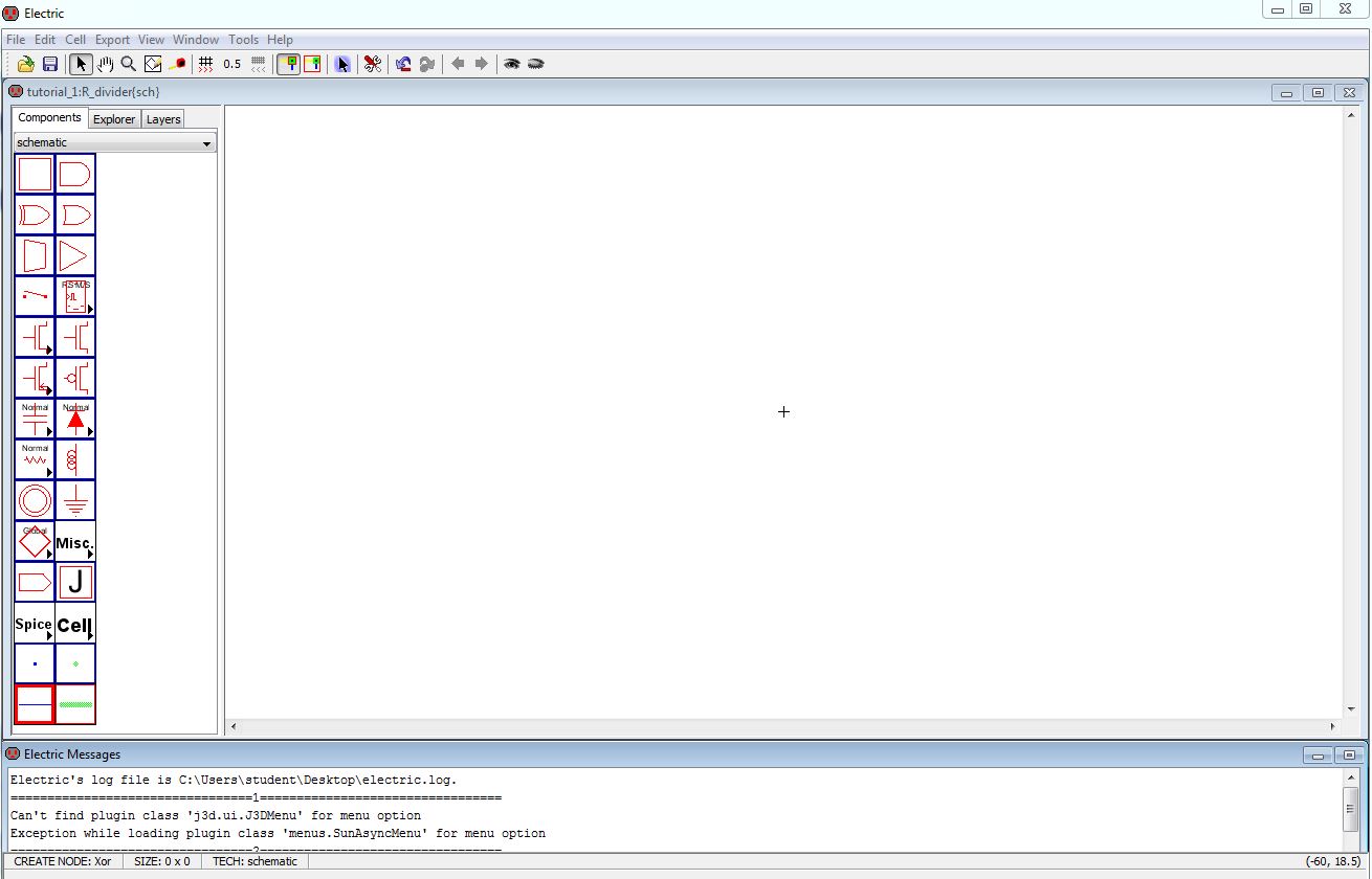
First, install and open Electric. You will will see the window below.
To make it easy to see what your doing lets change the background color to white.
You can do this by selecting Window -> Color Schemes -> White
Background Colors.
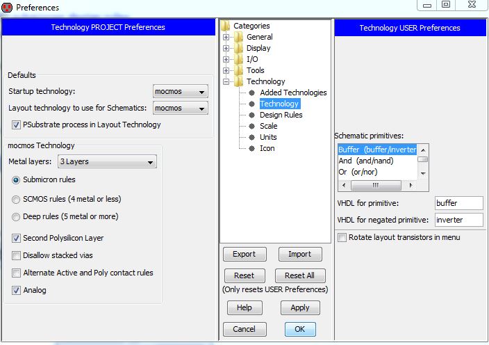
For this class we will set up Electric for use in ON semiconductor's C5 process and
fabrication through MOSIS. Select File -> Preferences (or just hit the
wrench/screwdriver menu icon) then Technology -> Technology to get to the
window seen below
Change the infomation to match what is seen below.
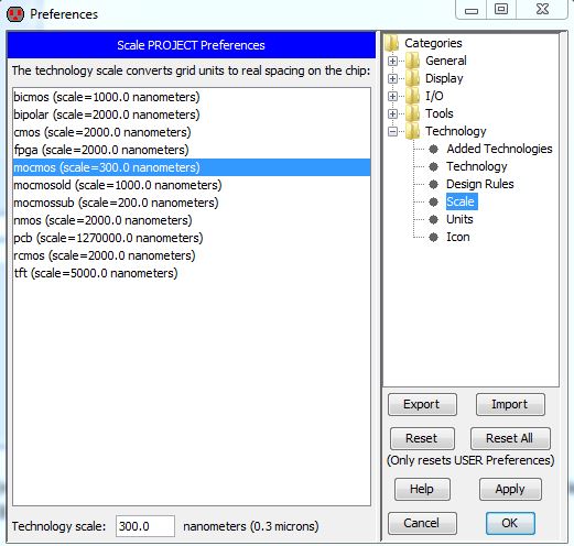
Next, goto scale and change the scale to 300 nanometers, This is done by typing in 300 at the bottom of the window.
Press OK and exit. A new window will pop up, select Mark All Libs.
Here are my Dr. Baker's peferences (right click and save as), electricPrefs.xml which can be loaded if there are
problems or to ensure consistency through the remainder of the tutorial.
Select File -> Import -> User Preferences followed by
navigating to where my preferences were saved imports these preferences if
there are problems.
Go to File -> Save Library As -> tutorial_1.jelib
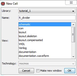
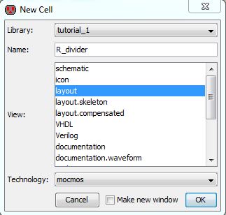
Next, go to Cell -> New Cell and enter the cell name (R_divider) and
view (schematic) seen below.
Hit Ok, select the component tab on the left side of the window.
In the component tab select the resistor symbol with the word "Normal" on it.
Slect the N-Well schematic resistor Node. Place the resistor on the schematic by left click on mouse.
Use the window menu to zoom in/out or fit.
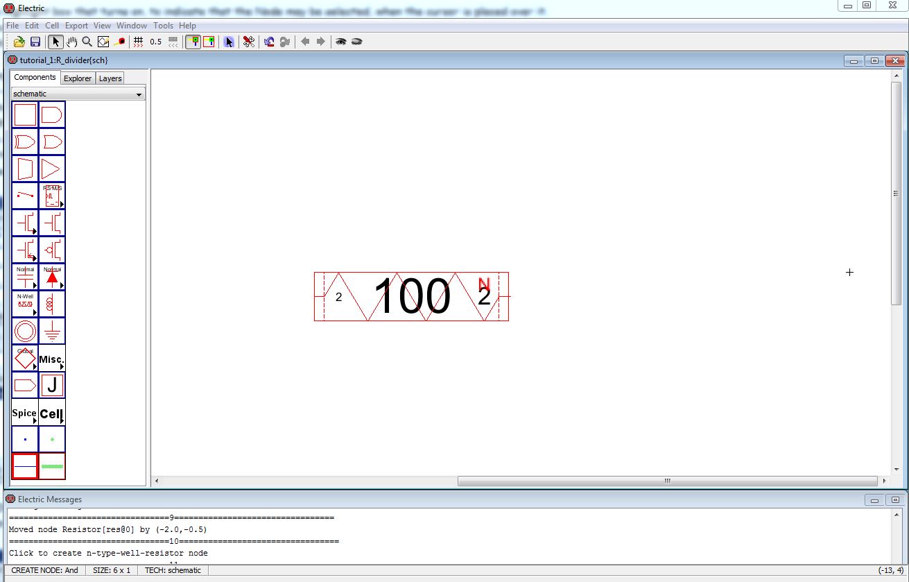
Select, by clicking on Node, the N-Well resistive Node.
Next go to Edit -> Properties -> Object Properties (or
simply Ctrl+I) to edit the properties of this Node
Match the window as shown below. (select more to view bottom portion of window)
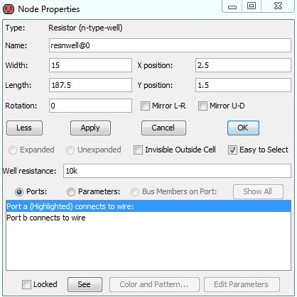
Hit OK.
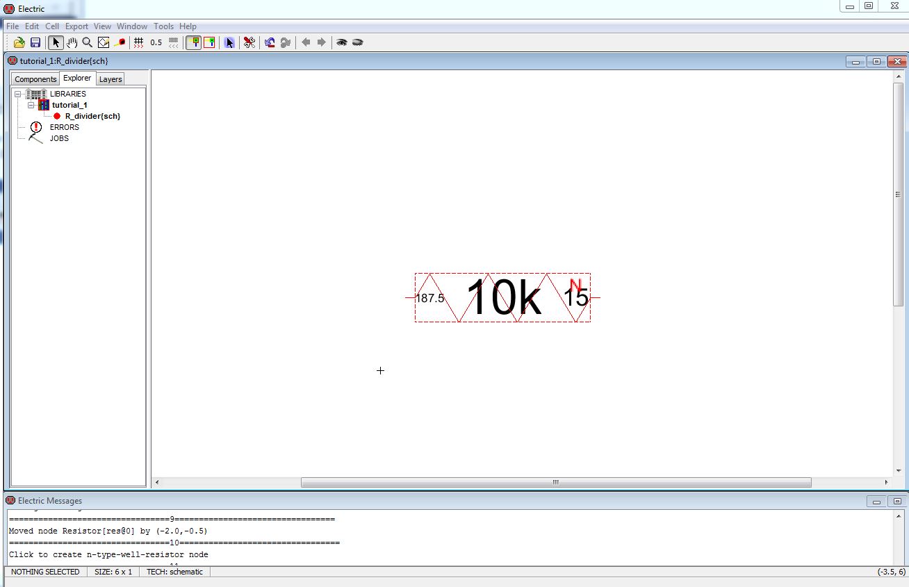
Go to Tools -> DRC -> Check
Hierarchically (or just hit F5) to check the schematic for errors.
These can be viewed on the bottom message window.
Let’s next make a layout corresponding to this schematic-view
cell.
Once more go to the menu item Cell -> New Cell and enter the
Name and View seen below.
2. Creating a backup
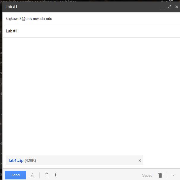
Create your lab folder on the desktop, you will want to work from this folder.
When
your all finished, zip the file (right click on your desktop
icon->send to->compressed file) and email it to yourself.
Retuern to EE421L Labs