Lab 10 – Final Project
EE 420L Analog IC Design
Lab Date: 4/24/19 Due: 5/08/19 at 5:30pm
Last Edited on
5/05/19 at 9:22am using Word
After reading,
reviewing, and practically building many different types of circuits in the
EE420 Analog Integrated Circuit Design Laboratory, we are ready to proceed to
do the final project.
In this lab,
we will be designing a Voltage Amplifier with at least a gain of 10 using
either the ZVN3306A or ZVP3306A MOSFETs, with as many resistors and capacitors
that we need. This will be a fast design, and be able
to drive a 1kΩ Load and have an Input Resistance greater than 50kΩ
and a large output swing as possible. We can also use AC coupling at the input
and the output of the amplifier, as long as we can
pass 100Hz.
The design
constraint is that our amplifier (with no input signal) can draw no more than
1mA from a 9V DC power source.
While building
this amplifier, it will be build
with the current condition as a high priority.
From studying
previous labs and reviewing informational text, the design will be using a
Push-Pull Amplifier:
In Lab 6, this
type of amplifier can give out one of the highest voltage gains with a very
large output swing that goes to about GND and VDD (assuming that the VDS,SAT and VSD,SAT are small).
The biggest drawback
is that there is no current-limiting resistor in the circuit and we would be
relying on the 1/gm resistance of the transistors. Since this amplifier gives
out a gain in the 60dB range, the Transconductance will be very large, meaning
that 1/gm will be a small resistance (possibly 10Ω), and thus there will
be a small resistance connecting from VDD to ground. This means we will have a
lot of current flowing through the circuit and we would need to use
current-limiting resistors at the top and bottom of the amplifer.
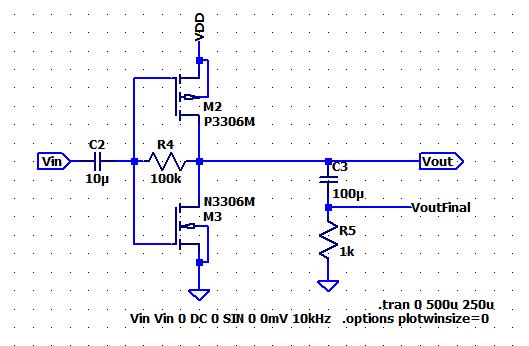
From the above
circuit, we get around ID = 168mA (oops) and a gm =
204mA/V (which means 1/gm = 5Ω!)
Lets add some resistors to our circuit:
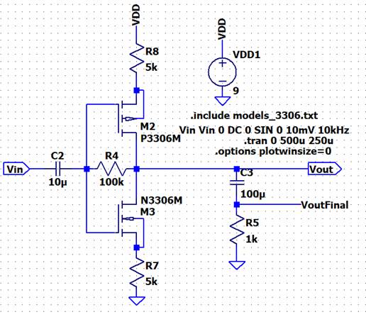
Assuming that we have around 10kΩ series
resistance in the branch (plus the higher 1/gm resistance from the MOSFETs) we
will get a much lower current of around 9Vx10kΩ = 1mA.
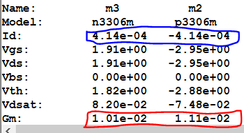
The
consequence of having less current through the MOSFETs is that we have a lower
gm and gains are decreased, especially when there is a small resistance at the
load that will kill the gain.
There are a
few things we can do to improve this. Suppose we have the Following Common
source amplifier:
Deriving the
gain equation for this topology we get:
Vin = Vgs + id(R2 || RSN) = id *
[ (1/gmN) + 1k||RSN ]
Vout = 0 – id*RD
Vout/Vin = (-1) [ RD ] /
[ (1/gmN) + 1k||RSN ]
= (-1) [ gm x RD ] /
[ 1 + (gm x 1k||RSN) ]
If we made RSN = 10Ω, then the parallel resistors
at the bottom of the NMOS would practically go to 10Ω (which also means
that the node would be near AC Ground) and thus we will have a much higher gain
at Vout.
With this in mind, if we add a parallel capacitor at the top
and bottom of the amplifier and try to pull the sources of the NMOS and PMOS to
AC Ground, we will get a similar outcome.
Now we have a
much better gain with the 1kΩ Load.
Now the
question comes: Why did we get this high increase of gain by pulling the
Sources of the MOSFETs to AC Ground?
Lets do some math:
AC Analysis:
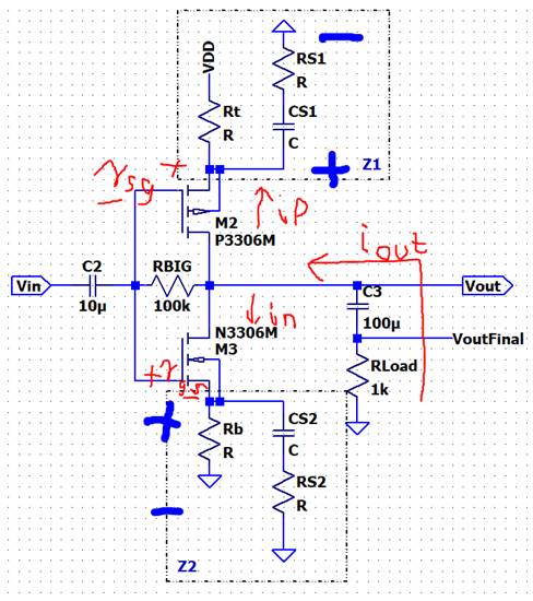
Assuming that the current in RBig
is 0, Z1 = Rt || (CS1 + RS1), Z1 = Rb || (CS2 + RS2)
IOut = In + Ip
VOut = 0 - (IOut
x RLoad)
Equation 1
(Going down and knowing Vgs = id / gmn = in / gmn):
Vin = Vgsn + In x Z2 = (In / gmn) +
In x Z2 = In x [ (1/gm) + Z2 ]
In = Vin / [ (1/gm) + Z2 ]
= [ gmn x Vin ] / [ 1 + (gmn
x Z2) ]
Equation 2
(Going Up and knowing that Vsg = id / gmp = -ip / gmp)
Note: id flows down from VDD to GND
Vin = -Vsg + Ip x Z1 = - (-ip /gmp) + Ip x Z1 = Ip x [ (1/gmp) +
Z1 ]
Ip = Vin / [ (1/gmp)
+ Z1 ] =
[ gmp x Vin ] / [ 1 + (gmp
x Z1) ]
Now With In and Ip,
Iout = In + Ip = {[ gmn x Vin
] / [ 1 + (gmn x Z2) ]} + {[ gmp x Vin ] / [ 1 + (gmp x Z1) ]}
Plugging this
into our Vout equation (and making it look nicer):
Vout = - ( {[ gmn x
Vin ] / [ 1 + (gmn x Z2) ]} + {[ gmp
x Vin ] / [ 1 + (gmp x Z1) ]}) x RLoad
Vout = - Vin x 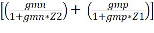 x RLoad
And thus, our
Voltage Gain for this Push-Pull Amplifier is:
AV = Vout / Vin = 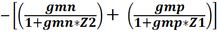 x RLoad
What this
means is that if we short the top and bottom impedances to AC ground (Assuming that
the capacitors are big enough to let AC flow through), then the bottom
denominator terms theoretically go to 1 and the gain will be:
Av = ![]() x RLoad
x RLoad
This looks
very familiar to the Gain equation of the Push-Pull Amplifier from Lab 6, where
the gain was determined by the transconductances times Rbig.
However, the load resistance will kill the gain to where the big resistance
would not make any difference in how
much gain we will get. [However if Rbig=0,
then it will definitely kill the gain :-( ]
Now with the
gain of the push-pull finished, the input resistance will be:
Rin = Vin / Iin
For that,
suppose we have this simple circuit model (for viewing purposes):
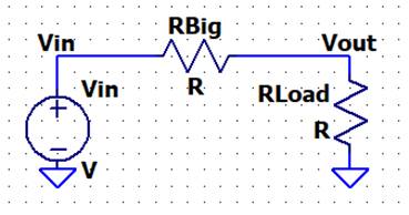
Iin = [ Vin – Vout ] / RBig = [ Vin – AV
x Vin ] / Rbig = Vin x [ 1 – AV ] / Rbig
Plugging this
current into our Rin equation and assuming AV = 11:
Rin = Rbig / [ 1 – AV ] = Rbig / [ 1 – 11
]
= - Rbig/10
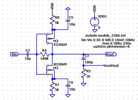
Now for the
amplifier design, suppose we would like to do a pre-amplifier stage for our
Push-Pull Amplifier. A two-stage amplifier is great because the first stage
helps to drive the input signal into the second stage so that the Load
Resistance does not kill the gain too much and also
the gain equation for the amplifier will be:
AvTotal = A1 x A2
For the
preamplifier stage, lets use a Common-Source Amplifier:
With this
stage, we will not only have a higher gain, but the input resistance will not
be a function of a gain but rather as a parallel combination of the two
resistors at the gate of the first stage amplifier.
The last plus is
that we can increase the Resistances of the first amplifier by a ratio and the
current can go down but the gain will not since the
gain is greatly changed by the small resistor at the capacitor. (And plus
the math is a bit nicer at the end)
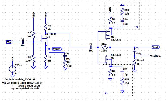
Designing so
that there is a gain of 10 V/V and that there is less than 1mA of current:
LTSpice Sim:
The Gain from LTSpice = 10.6V
AC Frequency
Response:
At 10Hz, we
start to get 20dB = 10V gain
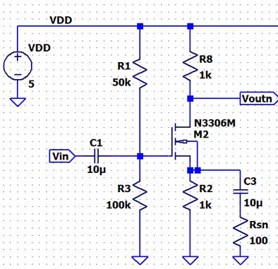
Hand Calcs :
Characteristics of the Transistor: KpN = .1233A/V2, W/L Ratio= 1, VTHN =
1.824 V
VG
= 9V (100k) / (100k + 100k) = 4.5V
ID
in the Gate Resistors = (4.5V)/100k = 45μA
ID
= Vs/110k = (1/2) Kp (W/L) (VGS – VTHN)2
= (1/2) (.1233) * (1/1) * (4.5 – VS – 1.824)2
Vs/6.78k = Vs2
– 5.352Vs + 7.16
Solving For Vs:
Vs = 2.71V,
2.64V
Solving for
the 2 possible VGS equations (So VGS >= 1.824V)
VGS1
= 4.5 - 2.71 = 1.79V, VGS2 = 4.5 – 2.64 = 1.86V
Finally,
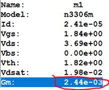
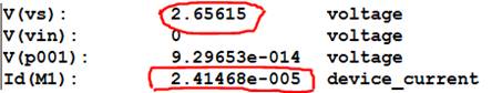
ID = 2.64V / 110kΩ = 23.4μA
Gm = (Kp) * (W/L) * (VGS – VTH) = (.1233) * (1/1) * (1.86 – 1.824)
Gm = 4.5mA/V
Rinput of Amplifier: 100k||100k = 50kΩ
LTSpice:
Looking at
this, our Hand calcs and Simulations look great!
Now for the
Second-Stage Amplifier, the Transconductance parameter is:
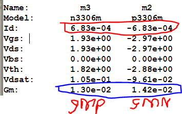
Gmp = 13mA/V Gmn = 14.2mA/V, ID
= 683μA
With the Transconductance,
we can finally find out the gain of The Push-Pull Amplifier
Input
Resistance into Second stage Push-Pull Amplifier :
Rin = Rbig / [ 1 – AV2 ] =
100k / (1 – Av2)
Gain of Av2 (With
test voltage Vin of 1VAC) =
AV2 = Vout / Vin = 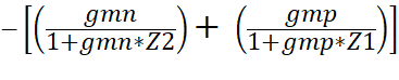 x RLoad
= 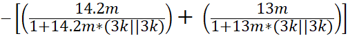 x 1kΩ
x 1kΩ
= -1.27 V/V Push-Pull Gain
Rinput of Push-Pull = 100k / (1 – (-1.27)) = 44.1kΩ Input Resistance
Gain Equation
of First Stage:
Vin = Vgs + id(R2 || RSN) = id *
[ (1/gmN) + R2||RSN ]
Vout = 0 – id*RD || Rinput
Vout/Vin = (-1) [ RD ||
Rinput] / [ (1/gmN)
+ R2||RSN ]
= - [ 110k || 44.1k ] /
[ (1/4.5m) + 110k||3.5k]
= - 8.7 V/V Common Source Gain
So the overall
Hand-Calculated Gain of the Amplifier is:
AvTOTAL = Av1 x Av2 = (-8.7V) x
(-1.27V)
= +11.05 V/V 2-Stage Gain (Non-Inverting)
So comparing this gain to our LTSpice gain
again:
We can verify
that all theoretical calculations work.
The last
condition is to check the DC Current:
Current at the
Gate Resistors of Input = 45μA
Current in
First MOSFET stage = 23uA
Current in
Second MOSFET stage = 683μA
Total Current =
751μA
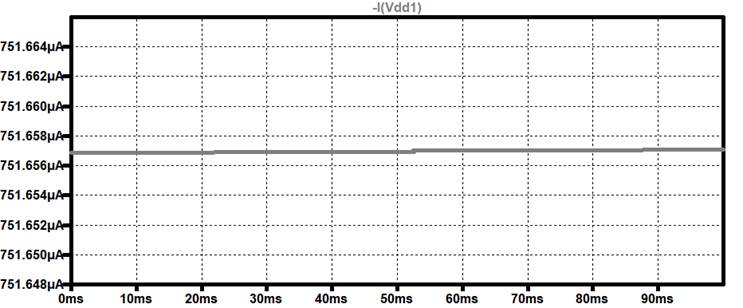
From this, we
have met all of the requirements of the Lab Project.
--------------------------------------------------------
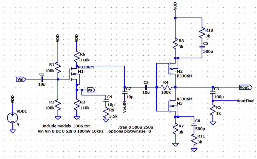
Experimental Results:
Note: Some Resistor values were changed
so that we can get a gain of 10 V/V
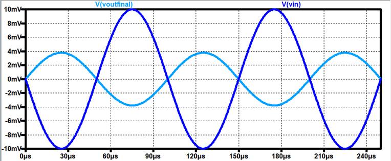
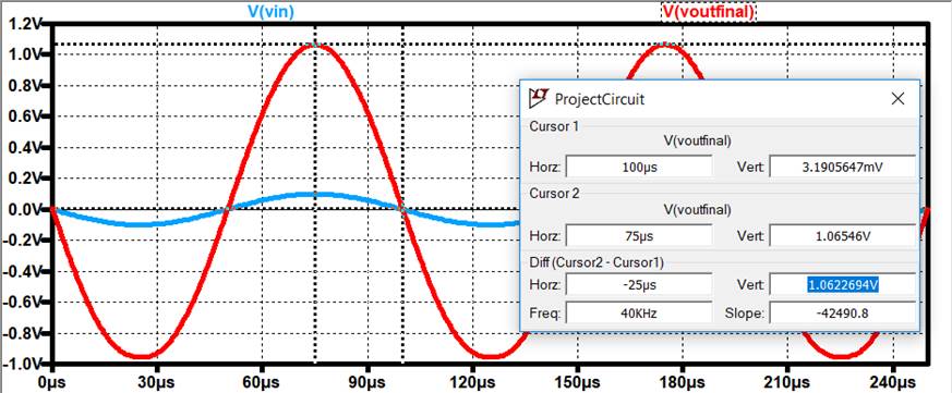
Voltage Gain
(At 100Hz):
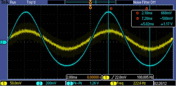
Vout / Vin = 11.7 V/V (Non-Inverting due to a 2-stage amplifier)
From this, we
meet the required gain at 100 Hz.
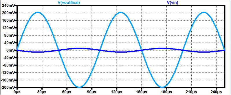
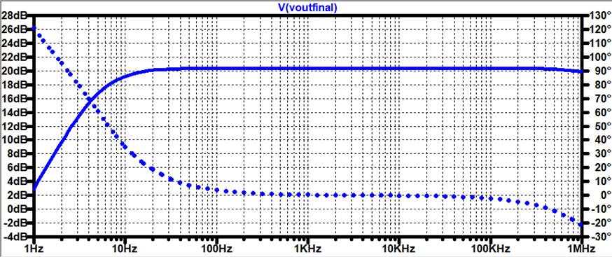
Frequency
Response:
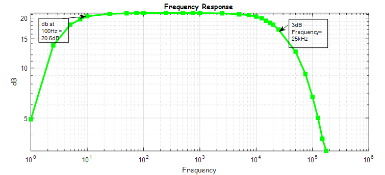
Looking at
this plot, the high frequency pole is near 20kHz, which at a practical stance
(suppose you were to build a speaker system, and the Human Ear can hear from
20Hz to 20kHz) is a good speaker amplifier.
Maximum Vout Swing:
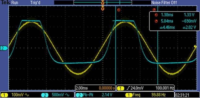
From this, we
can see that we have a 2V output swing, and thus we can have a Vin of around
200mV before it starts to clip.
Here is a pic
of a 200mV input AC voltage:
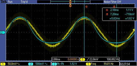
From here, we
still have a good gain, but this is the point where Vout
will start to clip.
The input
Resistance of the Amplifier can be found by placing a resistor at the input and
measuring the voltage drop across that resistor.
Inputting a 50kΩ
Resistor:
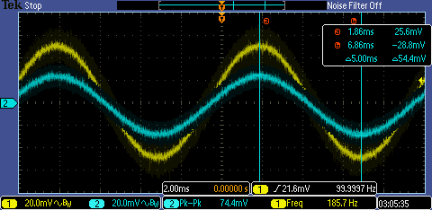
Knowing that:
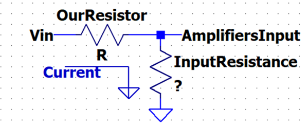
Solving for
the total current and doing the Amplifier Input Voltage divided by the Current:
[Vs – Vinput] / 50kΩ = [100mV – 54.4mV] / 50kΩ = 912nA
into Amplifier.
Amplifier
Input Resistance = 54.4mV / 912nA = 59.6kΩ
This Value is
close to our 50kΩ Theoretical Value, but it also passes the required
50kΩ input resistance requirement.
For learning
enhancement, here is the slew rate of the Amplifier:
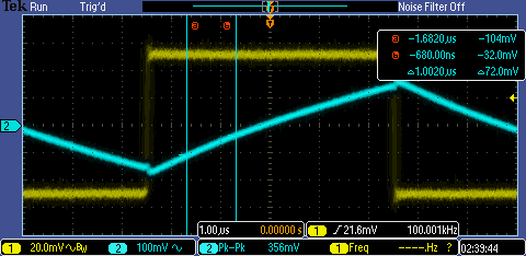
From this we
can see that we have a 72mV/μs slew rate.
The final
requirement is the Current that the amplifier draws.
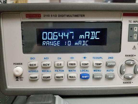
From this, we
are below the 1mA current and have a current that is around the hand-calculated
current.
--------------------------------------------------------------
Conclusion:
The Low-Power Amplifier
has shown me that there are many characteristics that must be taken account of
such as how the gain equations are strongly dominated by having a heavy (small)
resistor at the output. Also, learning to design (and experimentally test) a
two-stage amplifier has shown me that there is nothing hidden (no magic), and
that hand-calculations can prove to be near what the experimental results look
like.
The Analog IC
design Laboratory has taught me skills that will help with future research or in
the Industry. From characterizing CMOS Transistor Trays to compensating a scope
probe, this lab class has shown me that there is much more to learn and many things
that can enhance (and worsen) designs in microelectronic circuits.
-
Sources:
CMOSedu.com accompanied with: CMOS –
Circuit Design, Layout, and Simulation