Lab 7 – Design of an Audio Amplifier
EE 420L Analog IC Design
Lab Date: 3/27/19 Due: 4/03/19
Last Edited on
4/03/19 at 3:03pm using Word
From the
previous lab, we took a look into how we can take
small AC voltage signals and amplify them to bigger signals. In this lab, we
will be building a practical amplifier; an Audio Amplifier. The requirements of
this lab are to use a speaker that is in the range of 8-25Ω, and to use one 10μF Capacitor and one 100μF
Capacitor.
For this, we
will take a look at the Push-Pull Amplifier:
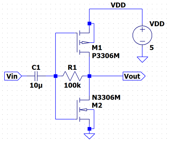
We will use
this amplifier because based off Lab 6, placing a small input signal at the
input of the amplifier will scale up our output by a huge factor that is mainly
dependent on the Resistance between the gate and drains of both the NMOS and
PMOS.
From Lab 6:
I = IN - IP
IN = gmN * Vgs = gmN * (Vin –
0)
IP = gmP * Vsg = gmP * (0 –
Vin)
[ Vin – Vout ] / R = [ gmN *
Vin ] – [ - gmP *Vin ]
- Vout / R = Vin ( gmN + gmP – 1/R)
Vout / Vin = - [ R * (gmN + gmP) ] + 1 = - [ R * (gmN + gmP) ]
Suppose, we would like to define our own parameters: We will be using an
input resistance of 2kΩ (so that we can get most of our AC voltage at the
input of the amplifier), a 20kΩ at the gate-drains of the MOSFETs, and inputting an 25Ω speaker.
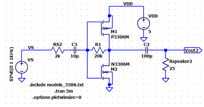
Since a small
resistor is at the output of the amplifier, the output resistance will
significantly decrease, meaning our AC output will be pulled even lower to
ground and thus, less gain than we anticipated. The DC Biasing will be the same
for the last lab, since the capacitors at the amplifier will isolate any DC
from both the input and the output of the amplifier.
For the DC
Bias Current: (Given Kpp = .145, Kpn
= .1233, VTN = 1.824V, VTP = 2.875)
IDN = IDP
(1/2)kpn*(VG – VTN)2 =
(1/2)kpp*(5-VG-VTP)2
VG-VTN =
sqrt(kpp/kpn)*(5-VG-VTP) K
= sqrt(kpp/kpn) = 1.0844
VG = K(5 – VTP) + K*VG + VTN
VG(1 + K) = K(5 – VTP) + VTN
VG = [ K(5 – VTP) + VTN ] / (1 + K) = [
1.0844(5 – 2.875) + 1.824 ] / (1 + 1.8044)
VG = 1.98V
VGSN =
1.98V, VSGP =
3.02V
ID =
(1/2)(.1233)*(1.98 – 1.824)2 = 1.52mA
LTSpice:
Now the
transconductance (AKA the gm) of the MOSFETs:
GmN = (.1233)*(1.98 –
1.824) = 19.3mA
GmP = (.145)*(3.02 – 2.875)
= 21mA
For the AC gain, it will change since now we will
consider the resistance at the output. Our new picture will look like:
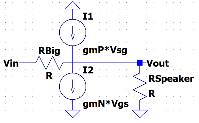
Assuming that the RO of the MOSFETs are
huge:
Vsg = -Vin, Vgs
= +Vin
KCL:
[ ( Vin – Vout ) / Rbig ] + gmP*Vsg = gmN*Vgs + [ Vout / Rspeaker ]
[ ( Vin – Vout ) / Rbig ] - gmP*Vin = gmN*Vin + [ Vout / Rs ]
Vout [ (1/RBig) - (1/Rs) ]
= - Vin [ gmP + gmN – (1/Rbig) ]
Vout / Vin = (-1) | [ gmP + gmN – (1/Rbig)
] / [ (1/RBig) - (1/Rs) ]
Vout / Vin = (-1) | [ 19.3m + 21m – (1/20k) ]
/ [ (1/20k) - (1/25) ]
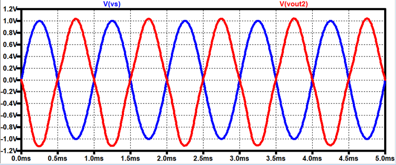
Vout / Vin = - 1.01 V/V
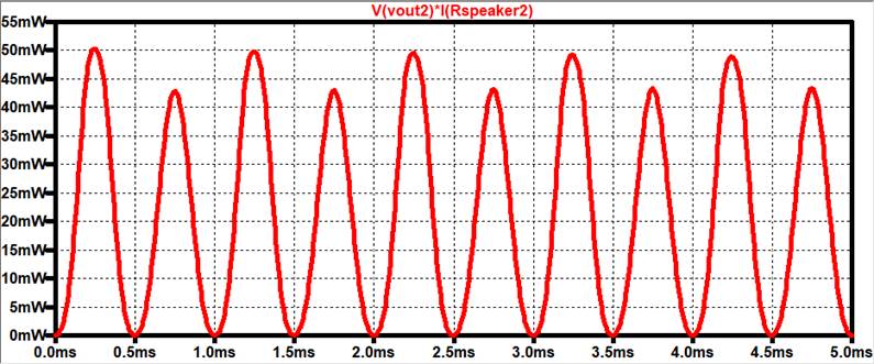
Max power from
Speaker:
P = V2
/ R = 12 / 25 = 40mW
LTSpice:
Here is the
power inside the speaker from LTSpice:
Power from Mosfet:
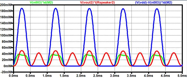
Blue is PMOS,
Green is NMOS, Red is Speaker.
Now that we
have our output, we can test our design:
We will use
the circuit shown above.
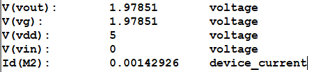
The output:
Gain = -272mV / V
There is a big
issue when it comes to connecting a load to the output.
From the last
lab, theoretically, if you place a capacitor at the output and insert a very
small resistance (so a wire) to ground, the AC voltage will go down
theoretically to 0. As we insert a small speaker, it will bring the original
gain of over 1k V/V to around a very small gain. The next approach was to build
a current amplifier such as the Source Follower, but
doing so will add another capacitor and we will not be within the requirements
of the lab.
The Power
dissipation of the speaker will be:
P = V2
/ R = .2722 / 25 = 2.95mW
We are not
really getting the output that we wanted, but we can see that we are outputting
what we do hear on the speaker.
The biggest
problem was that the MOSFETs were getting hot over a period
of time. From LTSpice, we are getting a high
wattage inside the PMOS and that was getting very hot. From the datasheet:
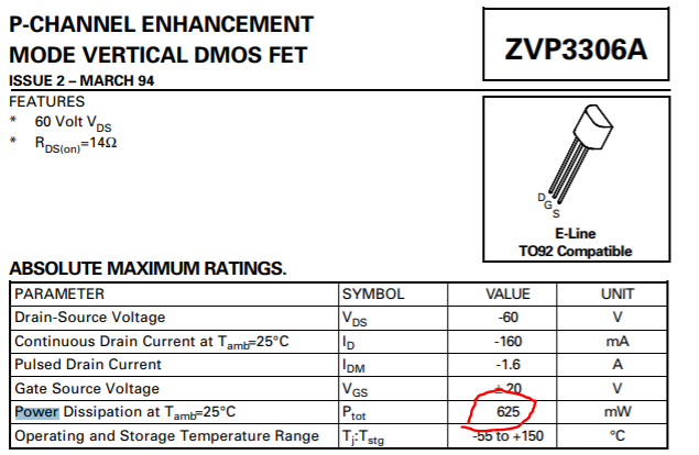
The power that
is actually through the PMOS is getting to the Max
power dissipation. We also lose a lot more power through the PMOS than we do
through the speaker. In a future (due to time), we could use some resistors at
the sources of the MOSFETs so that the voltage drop is lower between the MOSFETs.
Conclusion:
In the end,
the output of the Push-Pull Amplifier can theoretically give us a huge gain, but adding a very small resistive speaker at the output
will dramatically bring down our gain.
The output
resistance at the end will be determined by:
Rout =
Resistance of PMOS || Resistance of NMOS || Resistance of Speaker
Rout =
Resistance of Speaker.
The speaker will
be the dominant part of the gain and this will significantly reduce the output
voltage. In a future lab where we can use much more capacitors, we can build
the push pull amplifier followed by a Source Follower so that we can have a
first stage that amplifies the voltage and a second stage that amplifies the
current so that the speaker can work.
Here is a
quick video of our results.