Lab 6 – Single-Stage Transistor Amplifiers
EE 420L Analog IC Design
Lab Date: 3/13/19 Due: 3/27/19
By David Santiago – Email: santid4@unlv.nevada.edu
Last Edited on
3/25/19 at 10:06 pm using Word
Lab
description:
Throughout
most of the EE 420 Lectures, we have been discussing about
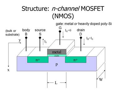
Metal-Oxide-Semiconductor Field-Effect Transistors, or MOSFETs for short.
MOSFETs consist of one big well of a specialized material of silicon, usually
referred as doped silicon. Within the well, are 2 smaller pockets of very
highly doped silicon, and the polarity is the opposite of the well. A negative
polarity is silicon usually doped with Phosphorus, which has more electrons in
the outer shell of the atom, and a positive polarity is silicon doped with
Boron, which has fewer electrons. A combination of these 2 doped regions will
give us a MOSFET.
In this lab,
we will be using both PMOS and NMOS transistors and working with Single-Stage
Amplifiers. 6
--------------------------------------------------------------------------------------------
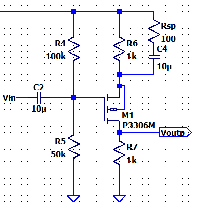
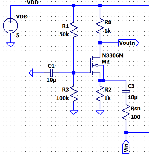
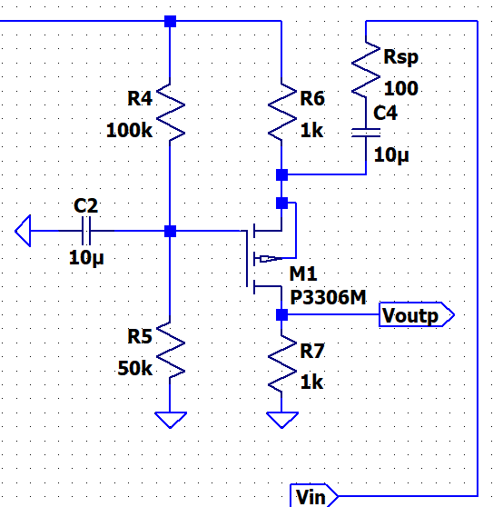
Experiment 1: Source Follower
Amplifier
We will be
looking at the NMOS and PMOS Source Follower (Or Common-Drain Amplifiers). These kind of circuits are called Common-Drain because the
Gate is where the input signal goes, the source is the output and the drain is
common “ground” to both. It is called a Source-Follower because the source (the
actual input) flows through into the output as is in phase.
We will first look at the NMOS Source Follower (using the
ZVN3306A):
Characteristics
of the Transistor: KpN = .1233A/V2,
W/L Ratio= 1, VTHN = 1.824 V
Hand Calcs:
VG = 5V (100k) / (100k +
50k) = 3.333V
ID = VS /
1kΩ
ID = (1/2) (Kp) * (W/L) * (VGS – VTH)2
= (1/2) (.1233) * (1/1) * (3.333 – VS – 1.824)2
Setting the two ID eqns equal to each other and doing
some math:
VS / (61.65) = VS2
– 3.019VS + 2.278
Solving for VS using the
Quadratic Eqn:
VS = 1.361V, 1.674V
VGS1 = 3.333 – 1.361 =
1.972V, VGS2 = 3.333 –
1.674 = 1.659V
Given our nice Inequality Equation: VGS
> VTHN = 1.824, the only acceptable answer is:
VGS = 1.972V
VS = 1.361V
Finally,
ID = 1.361 / 1k
ID
= 1.361mA
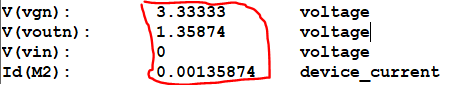
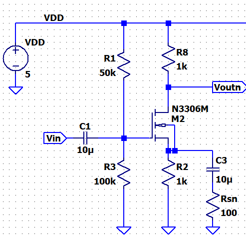
DC .op:
Time for the AC Analysis:
GmN
= (Kp) * (W/L) * (VGS – VTH) =
(.1233) * (1/1) * (1.972 – 1.824)
GmN = 18.2 mA/V
LTSpice Error Log
gm:
![]()
vgs
= vin - vout
id = vout
/ 1kΩ
vgs
= id / gmN = vout / [1k * gmN ] = vin
- vout
vout
[ 1 + 1k * gmN ] = 1k * gmN * vin
vout
/ vin = [1k * gmN ] / [ 1 + 1k *gmN ] =
[1k] / [ (1/gmN) + 1k ]
vout / vin = .948 V/V
Amplifier’s Resistances:
Rin = 50k || 100k = 33.33kΩ
Rout = (1/gmN) || 1k = 52Ω
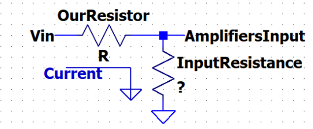
NOTE: We should learn some theory before we
proceed with experimentally finding the Input and Output resistances.
For the input resistance,
we are basically trying to create some voltage divider in which the first
resistor is our personal resistance, and the second resistor is the actual
resistance of the amplifier.
We cannot
really measure the Input resistance using an Ohmmeter, but we can use the
current through our pseudo-circuit, and solving for
the Input Resistance knowing the Voltage at the input of the actual amplifier
and the current into the amplifier.
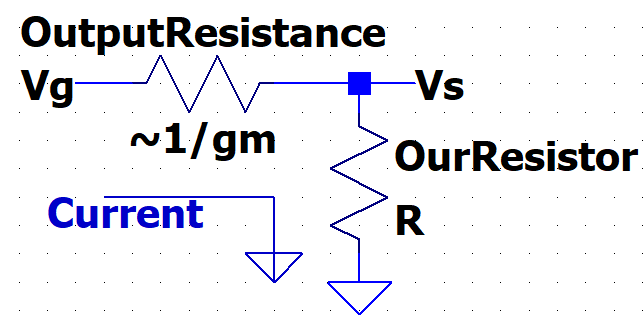
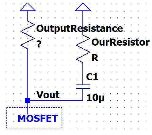
For the Output
Resistance, we will be also creating a pseudo-voltage divider circuit, where we
try to find the current through our own resistor at the output, and treating
the overall output resistance as the (1/gm) , since
(1/gm) || 1k is relatively equal to 1/gm. For that, we need the AC Vgs voltage and the current, which we can say is the
voltage through the resistor.
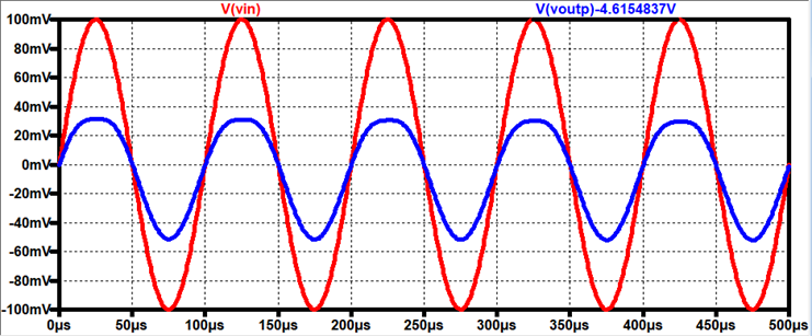
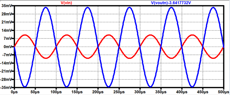
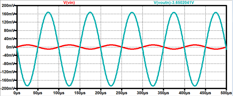
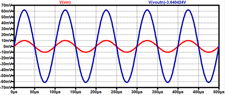
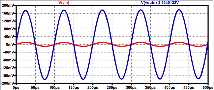
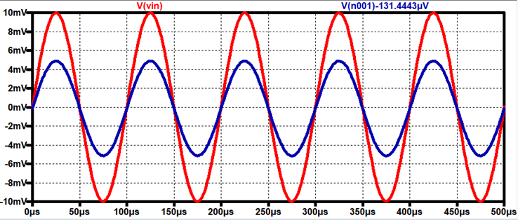
LTSpice:
Output:
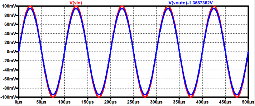
Gain = 0.95 V/V
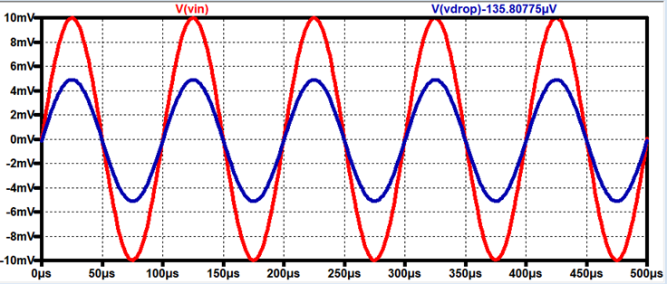
Input
Resistance Voltage Drop (using Rin = 33.33kΩ at Vin)
AC Voltage drop = 100mV – 50mV = 50mV
AC current through resistor = 50mV /
33.33kΩ = 1.5μA
Input Resistance of the Amplifier = 50m
/ 1.5μ = 33.33kΩ
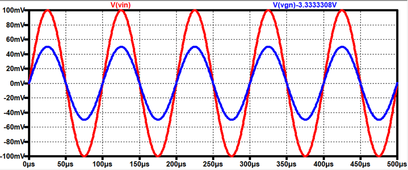
Output
Resistance Voltage Drop (Using Rout = 52Ω)
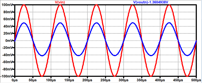
AC Voltage drop across Resistor = 50mV
AC Current through Resistor = 50mV /
52Ω = 0.961 A
Vg = Vin = 100mV, Vs = Voutn =
50mV
Vgs = 50mV
Output Resistance of the Amplifier = Vgs / id
Rout = 50m /
.961 = 52Ω
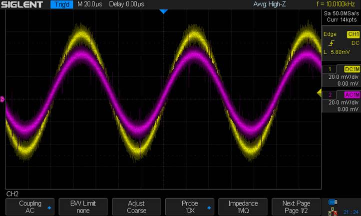
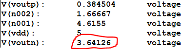
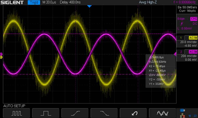
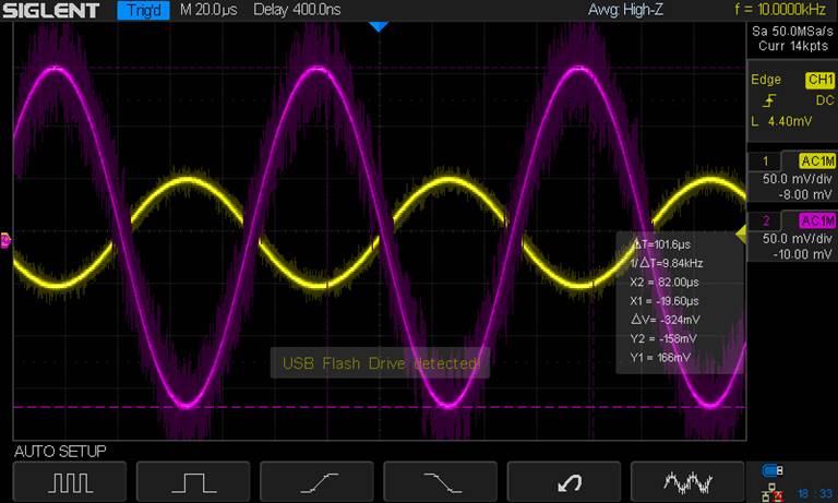
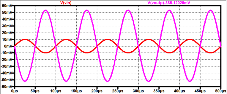
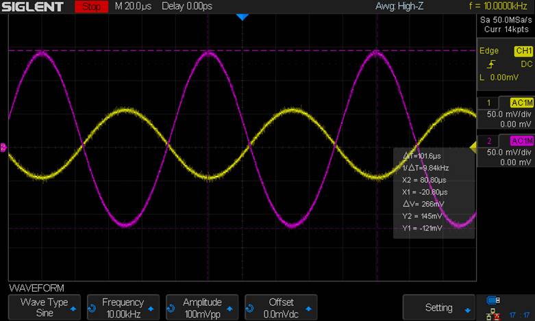
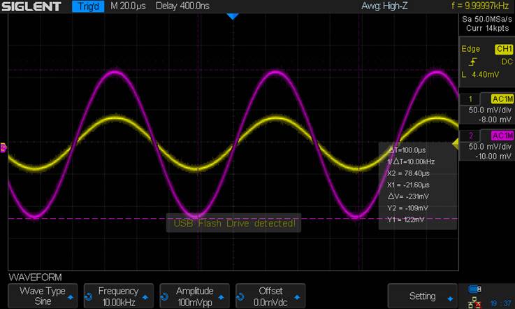
Experimental Results:
VoutN:
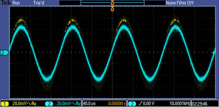
Gain =
.9 V/V
Input
Resistance (Using 33.3kΩ)
Voltage at Input Resistance = 62.8mV
AC Voltage drop through Resistor =
100mV – 62.8mV = 37.2mV
AC current through Resistor = 37.2m /
33.33k = 1.12uA
Input Resistance of the Amplifier =
62.8mV / 1.12μ = 56.1kΩ
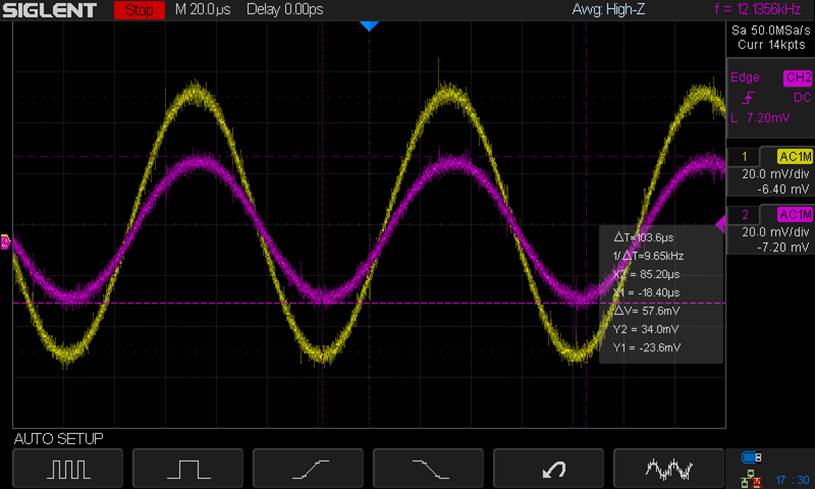
Output
Resistance (Using 52Ω):
AC Voltage Drop = 48.8mV
AC Current through Resistor = 48.8m /
52Ω = 0.938 A
Vg = Vin = 100mV, Vs = VoutN =
48.8mV
Vgs = 100m –
48.8m = 51.2mV
Output Resistance of the Amplifier = Vgs / id = 1/gm
Rout = 51.2m / .938 = 54.8 Ω
Table (So that
we can see our numbers):
|
NMOS |
Gain |
Rin |
Rout |
|
Theoretical |
.948 V/V |
33.33kΩ |
52Ω |
|
Experimental |
.95 V/V |
56.1kΩ |
54.8Ω |
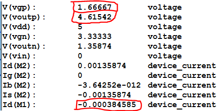
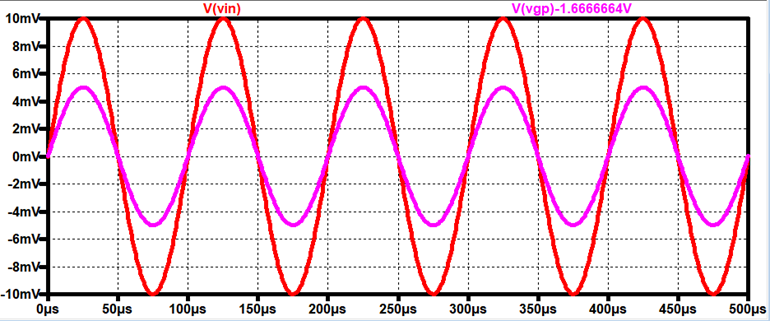
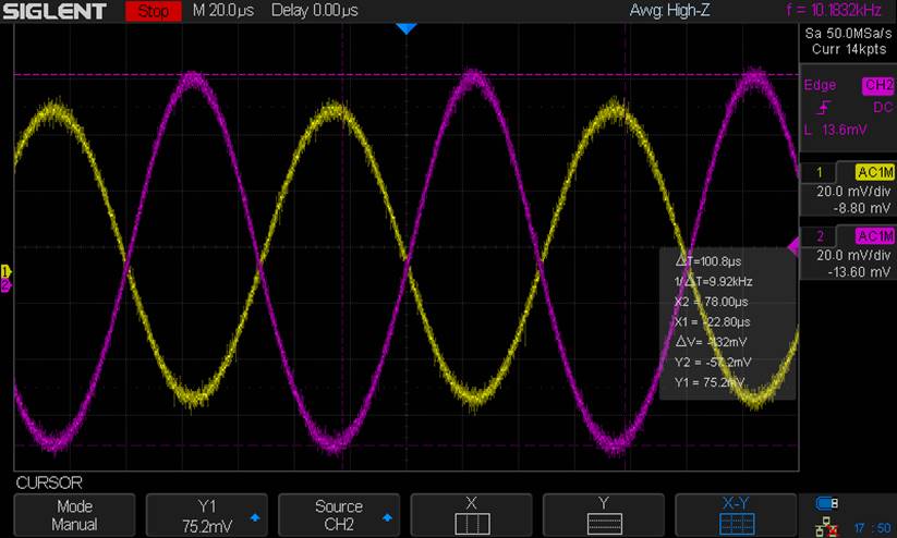
Now lets look at the PMOS (Using the ZVP3306A):
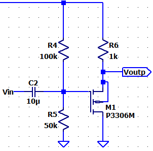
Characteristics
of the Transistor: KpP = .145A/V2,
W/L Ratio= 1, VTHN = 2.875V
Hand Calcs:
VG = 5V (50k) / (100k +
50k) = 1.667V
ID = [ 5 -VS ] / 1kΩ
ID = (1/2) (Kp) * (W/L) * (VSG – VTH)2
= (1/2) (.145) * (1/1) * (VS – 1.667 – 2.875)2
Setting the two ID eqns equal to each other and doing
some math:
[ 5-VS ]/
(72.5) = VS2 – 9.084VS + 20.63
Solving for VS using the
Quadratic Eqn:
VS = 4.613V, 4.456V
VSG1 = 4.613 – 1.667 =
2.946V, VSG2 = 4.456 – 1.667
= 2.790V
Given our nice Inequality Equation: VSG
> VTHP = 2.875, the only acceptable answer is:
VSG = 2.946V
VS = 4.613V
Finally,
ID = [5 – 4.613] / 1k
ID
= .346mA
DC .op:
AC Analysis:
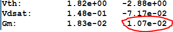
GmP
= (Kp) * (W/L) * (VSG – VTH) =
(.145) * (1/1) * (2.946 – 2.875)
GmP = 10.4 mA/V
Error Log:
vsg
= vout – vin
id = [0 - vout
]/ 1kΩ
vsg
= id / gmP = -vout / [1k * gmP ] = vout – vin
vout
[ 1 + 1k * gmP ] = 1k * gmP * vin
vout
/ vin = [1k * gmP ] / [ 1 + 1k *gmP ] = [1k]
/ [ (1/gmP) + 1k ]
vout / vin = 0.912 V/V
Amplifier’s Resistances:
Rin = 50k || 100k = 33.33kΩ
Rout = (1/gmP) || 1k = 87.7Ω
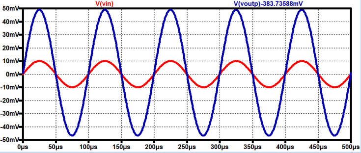
LTSpice:
Output:
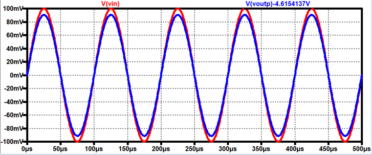
Gain = 0.9 V/V
Input Resistance
Voltage Drop (using Rin = 33.33kΩ at Vin)

AC Voltage drop = 100mV – 50mV = 50mV
AC current through resistor = 50mV /
33.33kΩ = 1.5μA
Input Resistance of the Amplifier = 50m
/ 1.5μ = 33.33kΩ
Output
Resistance Voltage Drop (Using Rout = 88Ω)
AC Voltage drop across Resistor = 50mV
AC Current through Resistor = 50mV /
88Ω = 0.568 A
Vg = Vin = 100mV, Vs = Voutn =
50mV
Vsg = 50mV
Output Resistance of the Amplifier = Vsg / id
Rout = 50m /
.568 = 88Ω
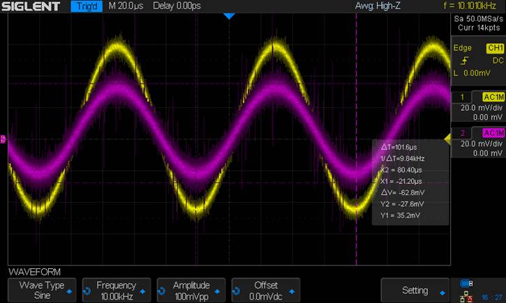
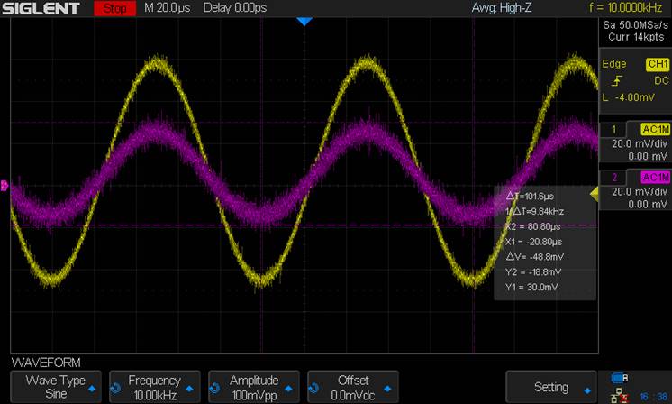
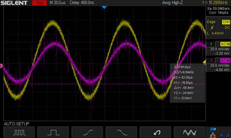
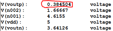
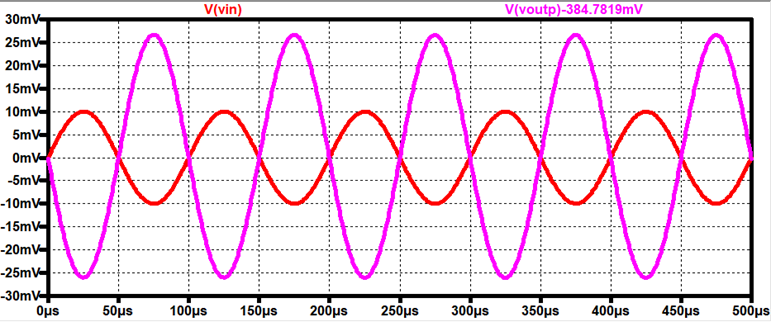
Experimental Results:
VoutP:
Gain =
.84 V/V
Input
Resistance (Using 33.3kΩ)
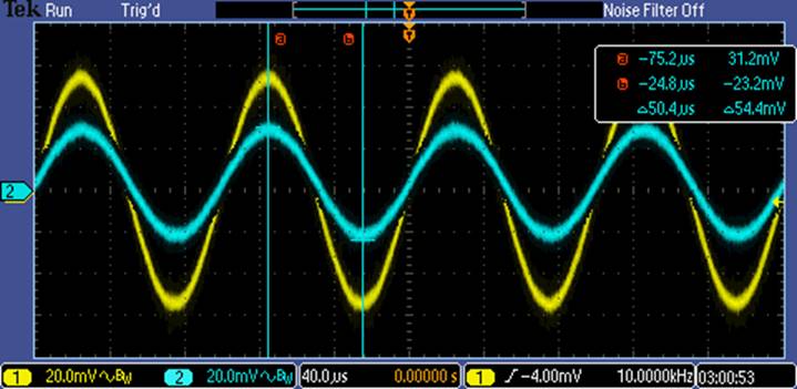
Voltage at Input Resistance = 54.4mV
AC Voltage drop through Resistor =
100mV – 54.4mV = 45.6mV
AC current through Resistor = 45.6m /
33.33k = 1.37uA
Input Resistance of the Amplifier =
54.4mV / 1.37μ = 39.7kΩ
Output
Resistance (Using 82Ω):
AC Voltage Drop = 26mV
AC Current through Resistor = 26m /
82Ω = 0.317 A
Vg = Vin = 100mV, Vs = VoutN =
26mV
Vgs = 100m –
26m = 74mV
Output Resistance of the Amplifier = Vgs / id
Rout = 74m / .317 = 233.4 Ω
Table :
|
PMOS |
Gain |
Rin |
Rout |
|
Theoretical |
.912 V/V |
33.33kΩ |
88Ω |
|
Experimental |
.84 V/V |
39.7kΩ |
233.4Ω |
------------------------------------------------------------------------------------
Experiment 2: Common-Source
Amplifier
We will now be
looking at the Common-Source Amplifier. It is called Common-Source since the
input is at the gate, the output is at the drain, and the source is common to
both the Input and Output.
Lets look at the
NMOS:
Hand Calcs:
NOTE: Since The gate resistance hasn’t
changed and neither has the resistor at the Source, we can say that the DC
biasing hand calcs are the same as the Source-Follower.
VG
= 3.333V, ID = 1.361mA, VGS = 1.972V
VD
= 5V – ID * 1k = 3.639V
DC .op:
AC Analysis:
Since gmN
is dependent on the DC biasing and the DC biasing for the common source amplifier
is the same as the Source Follower,
GmN
= 18.2 mA/V, 1/gm = 54.9Ω
Vin
= Vgs + id(R2
|| RSN) = id * [ (1/gmN)
+ 1k||RSN ]
Vout
= 0 – id*RD
Vout/Vin
= (-1) [ RD ] / [ (1/gmN)
+ 1k||RSN ] = [ 1k ] / [ 54.9 + 1k||100]
Vout / Vin
= -6.86 V/V
Amplifier’s Resistance:
Rin = 100k||50k = 33.33kΩ
Rout = 1k
LTSpice:
Output:
Gain = -6.7 V/V
Input
Resistance Voltage Drop (using Rin = 33.33kΩ at Vin)
AC Voltage drop = 10mV – 5mV = 5mV
AC current through resistor = 5mV /
33.33kΩ = .15μA
Input Resistance of the Amplifier = 5m
/ .15μ = 33.33kΩ
Output
Resistance Voltage Drop (Using Rout = 1kΩ)
NOTE: To solve for the output resistance,
there are 2 ways we can do this; we can use a resistor that is equal to the
resistance at the Drain, and see that VoutN will drop by 50%. We can then say that the AC current
that is pulled by the NMOS is the same, and the only difference is that the
current at the resistors is divided in half.
The second way
is by just looking at the circuit and saying “HEY, the output resistance is 1kΩ because there is a visible
1kΩ resistor at the output!”
AC Voltage drop across Resistor =
-33.5mV
Total AC Current through Amplifier =
-67mV / 1kΩ = -67μA
AC current through Resistor = -33.5mV /
1kΩ = -33.5mA
Current through Output Resistance = -67
+ 33.5 = -33.5mA
Output Resistance of the Amplifier = VoutR / iout = -33.5m/-33.5μ
Rout =
1kΩ
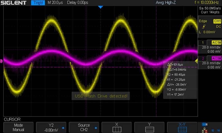
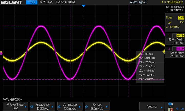
Experimental Results:
VoutN:
Gain =
-6.6 V/V
Input
Resistance (Using 33.3kΩ)
Voltage at Input Resistance = 58.4mV
AC Voltage drop through Resistor = 100mV
– 58.4mV = 41.6mV
AC current through Resistor = 41.6m /
33.33k = 1.25uA
Input Resistance of the Amplifier =
58.6mV / 1.25μ = 46.9kΩ
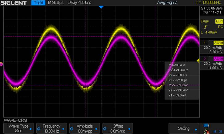
Output
Resistance (Using 1kΩ):
AC Voltage Drop = 325mV
From this, we can say that adding a
1kΩ resistor will divide the original output by half, or
Rout = 1kΩ
Table :
|
NMOS |
Gain |
Rin |
Rout |
|
Theoretical |
-6.86 V/V |
33.33kΩ |
1kΩ |
|
Experimental |
-6.6 V/V |
46.9kΩ |
1kΩ |
Question: What if we change RSN? What happens to the gain?
If we change
RSN, by the hand calcs:
vout/vin = (-1) [ RD ] / [ (1/gmN)
+ 1k||RSN ]
If RSN
decreases to 0Ω, then the 1k is shorted out, and then the gain increases
as the bottom term is decreased. If RSN is increased, then vice
versa, the gain will decrease but will be limited to the 1kΩ, and since
the 1kΩ will overpower (1/gm), Vout/Vin will
theoretically equal to -1V/V
At RSN = 0Ω, Gain = -16 V/V
At RSN = 1MEGΩ, Gain = -1 V/V
PMOS Time:
Hand Calcs:
NOTE: Just like in the NMOS case, the DC
biasing will be the same just like the Source Follower of the PMOS.
VG = 1.667V, VSG
= 2.946V, VS = 4.613V, ID = .346mA
VD
= ID * 1k = .346V
DC .op:
AC Analysis:
Just like in the NMOS, since our DC
biasing doesn’t change, gm doesn’t change.
GmP
= 10.4mA/V, 1/gm = 96.2Ω
Vin
= -Vsg - id(R2
|| RSP) = -id * [ (1/gmP)
+ 1k||RSP ]
Vout
= id*RD
Vout/Vin
= (-1) [ RD ] / [ (1/gmP)
+ 1k||RSP ] = [ 1k ] / [ 96.2 + 1k||100]
Vout / Vin
= -5.34 V/V
Amplifier’s Resistance:
Rin = 100k||50k = 33.33kΩ
Rout = 1k
LTSpice:
Output:
Gain = -5.32 V/V
Input
Resistance Voltage Drop (using Rin = 33.33kΩ at Vin)
AC Voltage drop = 10mV – 5mV = 5mV
AC current through resistor = 5mV /
33.33kΩ = .15μA
Input Resistance of the Amplifier = 5m
/ .15μ = 33.33kΩ
Output
Resistance Voltage Drop (Using Rout = 1kΩ)
AC Voltage drop across Resistor =
-26.6mV
Total AC Current through Amplifier =
-67mV / 1kΩ = -67μA
AC current through Resistor = -33.5mV /
1kΩ = -33.5mA
Current through Output Resistance = -67
+ 33.5 = -33.5mA
Output Resistance of the Amplifier = VoutR / Iout = -33.5m/-33.5μ
Rout =
1kΩ
Experimental Results:
VoutP:
Gain =
-2.66 V/V
Input
Resistance (Using 33.3kΩ)
Voltage at Input Resistance = 57.6mV
AC Voltage drop through Resistor =
100mV – 57.6mV = 42.4mV
AC current through Resistor = 42.4m /
33.33k = 1.27uA
Input Resistance of the Amplifier =
57.6mV / 1.27μ = 45.4kΩ
Output
Resistance (Using 1kΩ):
AC Voltage Drop = 132mV
From this, we can say that adding a
1kΩ resistor will divide the output by half, or
Rout = 1kΩ
Table :
|
PMOS |
Gain |
Rin |
Rout |
|
Theoretical |
-5.34 V/V |
33.33kΩ |
1kΩ |
|
Experimental |
-2.66 V/V |
45.4kΩ |
1kΩ |
What if we change RSP?
Just like in the NMOS
case, looking at the Gain equation for the Common Source:
Vout/Vin = (-1) [ RD ] / [ (1/gmP)
+ 1k||RSP ]
Decreasing the
RSP to 0Ω will create Maximum gain, and increasing RSP
to some resistance such as 1 MEG or infinity Resistance, the gain will
theoretically be equal to -1 V/V
--------------------------------------------------------------------------------------------
Experiment 3: The Common-Gate
Amplifier
NMOS:
Hand Calcs:
NOTE: The DC biasing will be the same as the
Source follower and the Common Gate amplifiers.
VG
= 3.333V, ID = 1.361mA, VGS = 1.972V VD =
3.639V
AC Analysis:
Because the DC biasing doesn’t change…
GmN
= 18.2 mA/V, 1/gm = 54.9Ω
Vout = 0 – id
* 1k
Vin = -id [ (1/gm)||1k + 100Ω ]
Vout / Vin = [ RD ] / [ (1/gm)||1k + 100 ] = [ 1k ] / [ (54.9)||1k + 100 ]
Vout / Vin = 6.58 V/V
Amplifier’s Resistance:
Rin = (1/gmN)||1k + 100 =
152Ω
Rout = 1k
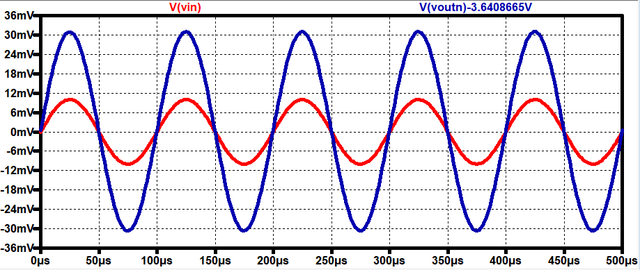
LTSpice:
Output:
Gain = 6.2 V/V
Input
Resistance Voltage Drop (using Rin = 152Ω at Vin)
AC Voltage drop = 10mV – 5mV = 5mV
AC current through resistor = 5mV /
152Ω = 32.9μA
Input Resistance of the Amplifier = 5m
/ 32.9μ = 152Ω
Output
Resistance Voltage Drop (Using Rout = 1kΩ)

AC Voltage drop across Resistor = 31mV
Total AC Current through Amplifier =
62mV / 1kΩ = 62μA
AC current through Resistor = 31mV /
1kΩ = 31mA
Current through Output Resistance = 62
+ 31 = 31mA
Output Resistance of the Amplifier = VoutR / Iout = 31m/31μ
Rout =
1kΩ
Experimental Results:
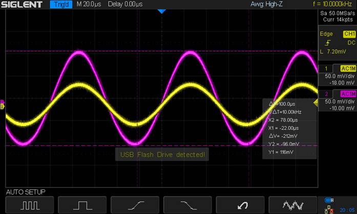
VoutN:
Gain =
4.66 V/V
Input
Resistance (Using 152Ω)
Voltage at Input Resistance = 69.2mV
AC Voltage drop through Resistor =
100mV – 69.2mV = 30.8mV
AC current through Resistor = 30.8m /
152 = 203uA
Input Resistance of the Amplifier =
69.2mV / 203μ = 342Ω
Output
Resistance (Using 1kΩ):
AC Voltage Drop = 231mV
Since this is half of our initial
Output gain, we can say
Rout = 1kΩ
Table :
|
NMOS |
Gain |
Rin |
Rout |
|
Theoretical |
6.58 V/V |
152Ω |
1kΩ |
|
Experimental |
4.66 V/V |
342Ω |
1kΩ |
What if we modified RSN?
For the common
gate, we can actually see a bit of a preview of what
happens to RSP when we were calculating the Input Resistance. By the
gain equation of the Common Gate:
Vout / Vin =
[ RD ] / [ (1/gm)||1k + RSN ]
Increasing RSN to a higher
resistance or even infinite resistance will lower the amplification of the
amplifier (and thus to 0 Gain at infinite Resistance). You can see that when we
were adding a resistance in series to RSP when we were calculating
the Input Resistance.
Decreasing it to where RSN is
something like 0Ω will result in an equation that will give us the maximum
amplification, which is:
Vout / Vin =
[ RD ] / [ (1/gm)||1k + 0] = 19.2 V/V
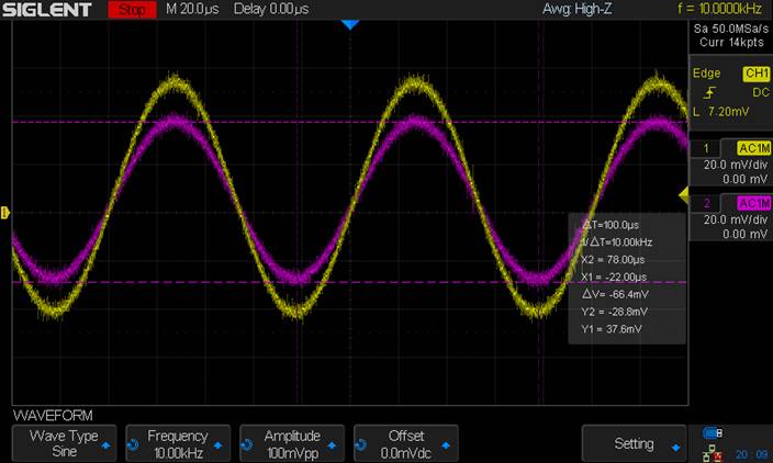
Here is a
quick simulation showing the max gain (With RSN = 0Ω:
Gain = 17.6 V/V
Introducing our PMOS Common Gate Amplifier:
Hand Calcs:
NOTE: The DC biasing will be the same as the
Source follower and the Common Gate amplifiers.
VG
= 1.667V, VSG = 2.946V, VS = 4.613V, ID =
.346mA, VD = .346V
AC Analysis:
Same ID as in previous PMOS,
GmN
= 10.4 mA/V, 1/gm = 96.2Ω
Vout = id
* 1k
Vin = +id [ (1/gmP)||1k
+ 100Ω ]
Vout / Vin = [ RD ] / [ (1/gmP)||1k
+ 100 ] = [ 1k ] / [ (96.2)||1k + 100
]
Vout / Vin = 5.33 V/V
Amplifier’s Resistance:
Rin = (1/gmP)||1k + 100 =
187.7Ω
Rout = 1k
LTSpice:
Output:
Gain = 4.9 V/V
Input
Resistance Voltage Drop (using Rin = 188Ω at Vin)
AC Voltage drop = 10mV – 5mV = 5mV
AC current through resistor = 5mV /
188Ω = 26.6μA
Input Resistance of the Amplifier = 5m
/ 26.6μ = 188Ω
Output
Resistance Voltage Drop (Using Rout = 1kΩ)
AC Voltage drop across Resistor =
24.5mV
Total AC Current through Amplifier =
49mV / 1kΩ = 49μA
AC current through Resistor = 24.5mV /
1kΩ = -24.5mA
Current through Output Resistance = 49
– 24.5 = 24.5mA
Output Resistance of the Amplifier = VoutR / Iout = 24.5m/24.5μ
Rout =
1kΩ
Experimental Results:
VoutP:
Gain =
2.12 V/V
Input
Resistance (Using 182Ω)
Voltage at Input Resistance = 66.4mV
AC Voltage drop through Resistor =
100mV – 66.4mV = 33.6mV
AC current through Resistor = 33.6m /
182 = 184.6uA
Input Resistance of the Amplifier =
66.4mV / 184.6μ = 359.7Ω
Output
Resistance (Using 1kΩ):
AC Voltage Drop = 101mV
Seeing that the Voltage dropped by
half,
Rout = 1kΩ
Table :
|
PMOS |
Gain |
Rin |
Rout |
|
Theoretical |
5.33 V/V |
188Ω |
1kΩ |
|
Experimental |
2.12 V/V |
359.7Ω |
1kΩ |
Suppose we change RSP:
By our gain
equation:
Vout / Vin =
[ RD ] / [ (1/gmP)||1k
+ RSP ]
If RSP
goes to infinity resistance, we theoretically will get a very small gain
(theoretically 0 V/V). You can see this voltage get smaller when we added a
resistor in series with RSP when we were calculating the Input
Resistance.
If RSP
decreases to something like 0Ω, we will get a Max gain of:
Vout / Vin =
[ RD ] / [ (1/gmP)||1k
+ 0 ] = 11.4 V/V
Here is a
quick sim to show this:
Gain = 10.5 V/V
-----------------------------------------------------------------------------------
Experiment 4: The Push-Pull Amplifier
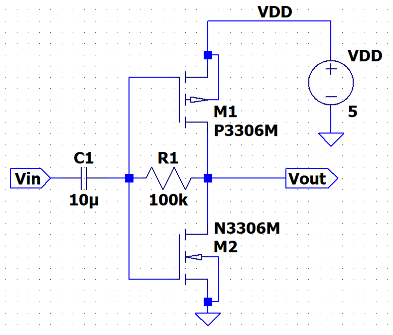
The push-pull
Amplifier is basically an amplifier that pushes and pulls current through our
Load Resistor R. If you think about it, the very Large R basically acts like an
Open, meaning that there is no current through the load, meaning that the
potentials at the gates of both MOSFETs are equal to the potentials at the
Drains of both the MOSFETs. In other words, the MOSFETs are always in
saturation. As current goes into the gates, the voltage at the gate goes Up,
and that will cause the NMOS to turn ON and the PMOS to turn OFF. As current is
sinked back into Vout, the
NMOS turns slightly OFF and the PMOS turns slightly ON. This continues on,
hence why its called a
Push-Pull Amplifier. This also implies that this amplifier is great at sinking
and sourcing current, and it is all dependent on the current that is running
through the load. The higher the load, the higher the gain!
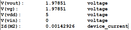
Hand Calcs:
Assuming that both
MOSFETs are in saturation,
IDN = IDP
(1/2)kpn*(VG – VTN)2 = (1/2)kpp*(5-VG-VTP)2
VG-VTN = sqrt(kpp/kpn)*(5-VG-VTP) K
= sqrt(kpp/kpn) = 1.0844
VG = K(5 – VTP)
+ K*VG + VTN
VG(1 + K) =
K(5 – VTP) + VTN
VG = [ K(5 – VTP)
+ VTN ] / (1 + K) = [ 1.0844(5 – 2.875) + 1.824 ] / (1 + 1.8044)
VG =
1.98V
VGSN = 1.98V, VSGP = 3.02V
ID = (1/2)(.1233)*(1.98
– 1.824)2 = 1.52mA
LTSPICE:
AC Analysis:
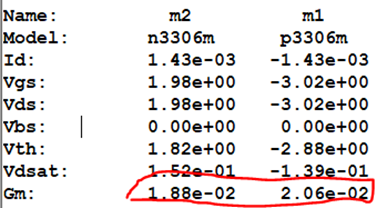
GmN = (.1233)*(1.98 – 1.824) = 19.3mA
GmP = (.145)*(3.02 – 2.875) = 21mA
LTSPICE:
AC Equivalent Circuit:
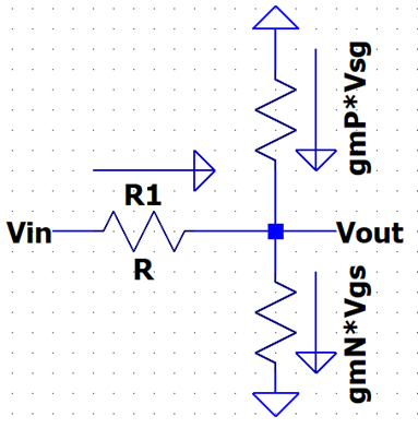
I = IN
- IP
IN
= gmN * Vgs = gmN * (Vin – 0)
IP
= gmP * Vsg = gmP * (0 – Vin)
[ Vin – Vout ] /
R = [ gmN * Vin ] – [ - gmP
*Vin ]
- Vout / R = Vin ( gmN
+ gmP – 1/R)
Vout / Vin = - [ R * (gmN + gmP) ] + 1 = - [ R * (gmN + gmP) ]
For the 100kΩ Case:
Vout / Vin = - 100k * (19.3m + 21m) = -4.03k V/V
LTSpice:
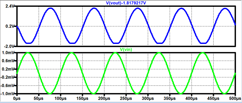
Gain = -2.4k V/V
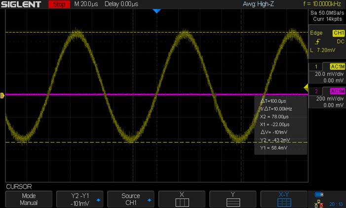
Experiment:
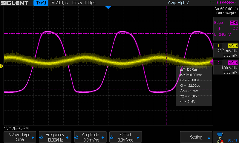
Gain =
-3.74 kV/V
For the 500k Case:
Vout / Vin = - 500k * (19.3m + 21m) = -20.15k V/V
LTSpice:
Gain = -3.5k V/V
Experiment:
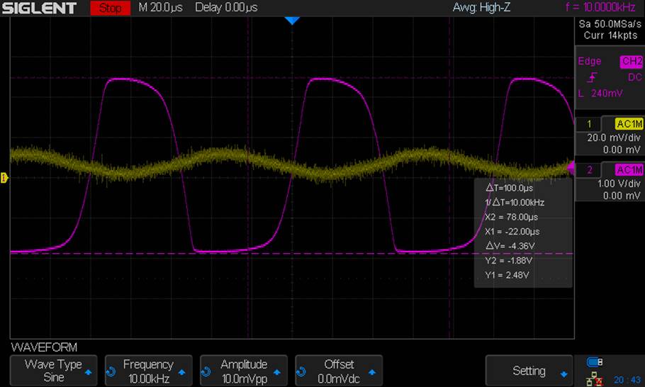
Gain =
-4.36k V/V
|
Resistance |
Hand Calcs |
LTSpice |
Experiment |
|
100kΩ |
-4.03k V/V |
-2.4k V/V |
-3.74k V/V |
|
500kΩ |
-20.15k V/V |
-3.5k V/V |
-4.36k V/V |
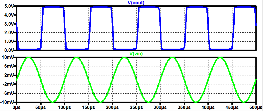
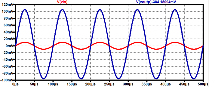
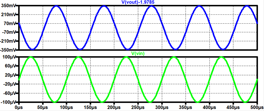
From this, we
can see that our output is wanting to rail to its max Vpp
of around 4~5Vpp, which is about the range of our 0 to VDD battery source. We
could of used a lower input signal voltage so that we
could see the whole signal, but we could not do this due to the oscilloscope
not wanting to read the lower input signals. To show that the amplifier is
railing to GND and VDD, here is a quick simulation of LTSpice
using 10mV input just like how we used it in our lab: (Using R = 100k)