Lab 5 – Op Amps III
EE 420L Analog IC Design
Lab Date: 2/27/19 Due: 3/13/19
Last Edited on
3/10/19 at 3:15pm using Word
The Op-Amp can
provide us with an output that will amplify whatever our input is. The kind of
amplification can differ with how you build the Closed-Loop gain of the Op-Amp.
In the Non-Inverting Op-Amp, we have a positive gain at our output, and in the
inverting Op-Amp, we will get a negative gain.
What if, using
the Inverting Topology, we wanted to remove the Resistor that is at the Output
and the inverting port of the Op-Amp with a capacitor?
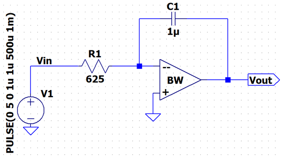
Assume that
the inverting and non-inverting ports are 0V, the output of the capacitor will
be:
Vout = 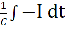 , I = [Vin(t) – 0] /R
Whatever our
signal will be, the output will be our input voltage scaled by 1/R over time.
In this lab, we
will be looking at the Integrator and be calculating its frequency response. We
will also be designing our own Integrator and give a specific output on the
Oscilloscope.
--------------------------------------------------------
Experiment 1:
Lets do some Algebra… Making R1 = Ri, R2 = Rf, ZC1 = 1/(jωC), and Vcm = 0,
Rf
|| ZC1
= [ Rf / (jωC)
] / [ Rf + 1/(jωC) ]
Parallel
Impedance = Rf / [ 1 + jω*Rf*C ]
[Vin – 0 ] / Ri = [ 0
– Vout ] * [ Rf + 1/(jω*Rf*C)
] / Rf
NOTE: Last part of
Right hand eqn is our Parallel Impedance
Vout / Vin =
Rf / [ Ri * (1 + jω*Rf*C) ]
Vout / Vin = (-1) / [ (Ri/Rf) + jω*Ri*C) ] , Our Frequency
Response
Given Ri = 1kΩ, Rf = 100kΩ,
and C = 1uF,
Vout/Vin = 1 / [(Ri/Rf) + j(ω*Ri*C)
]
|Vout/Vin| =
1 = 1 /sqrt([(Ri/Rf)2 + (ωf*Ri*C)2]
([(Ri/Rf)2 + (ωf*Ri*C)2]
= 1
F = sqrt[1
– (Ri/Rf)2 ] / [ 2πRiC ] = sqrt(1 – (1k/100k)2
) / [2π1k*1u]
FUn = 159.2Hz
the angle will
be:
180° - tan-1[wRiC /(Ri/Rf)] = 180 – 89.99999° = approx. +90°
If you wanted
to make life less painful, we can exclude R2 (100KΩ) since its impedance will be much
greater than the impedance of the Capacitor that R2 will behave like an Open.
So, Our new
equation (Assuming Rf = ∞ )
Vout / Vin = (-1) / [
0 + jω*Ri*C) ] ,
Frequency Response without Rf (or Rbig)
Angle |Vout/Vin|
= 180° (Top is negative) – 90°(bottom j) = +90°
Unity Gain Frequency:
|Vout/Vin| =
1 = 1 / [ 2πfUnity*Ri*C ], fUnity = 1 / [
2π*1k*1μ ] = 159.2 Hz
Removing the really big resistor made our calculations really nice, however
in practice, we need a big resistance there because if we exclude the big
resistor, there is a small DC offset voltage located at the Non-inverting
Terminal of the Op-Amp. By the Non-Inverting Equation, assuming Rbig = ∞
Vout = (VOffset) *( 1 + Rbig/Ri)
Our gain will
be infinity, meaning our small little DC offset will be amplified, and
depending on the polarity of the DC offset, the Output will either Rail to VCC-
(or GND) or it will Rail to VCC+ (or VDD = 5V). This is very important to know, especially for the next part of the lab,
and this will save a LOT of headaches. Shoutout to J. Skelly
In reality, the 100kΩ resistor does not have an
effect at all in our Frequency response. From doing the frequency with and
without the 100kΩ, our circuit should have FUN = 159Hz and at
90°. But in practice, we need that Big resistor so that we can suppress the VOffset, which we will talk about later.
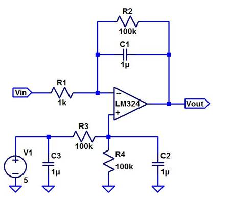
LTSpice:
Output:
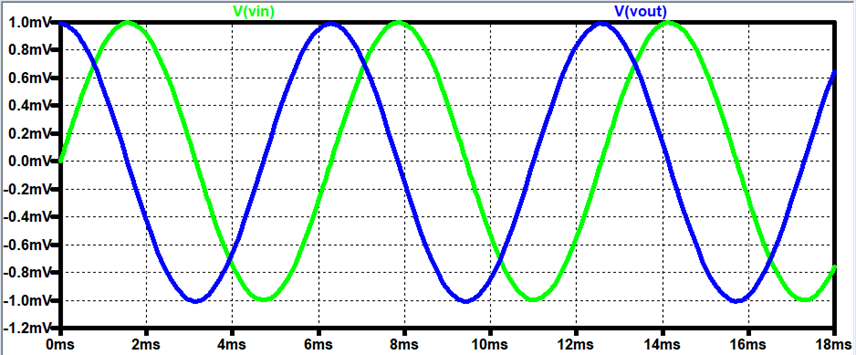
As you can
see, at 159Hz, we should theoretically get a gain of 1 and 90° phase shift.
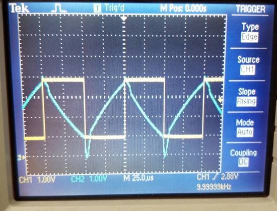
Experimental Stuff..
Lets prove our hand calcs…
Using just
about the same Resistors and capacitors (Also Vcm = 2.5V):
Output:
Looking at
this output, we can verify that our phase shift is what we expect: it is 90° from
the input and the output.
Experiment 2: Our Integrator
Lets build our very own integrator! From what we
learned, we can create a triangle wave from a square wave.
To derive our formuler, we will use our known equation for the Capacitor:
Change of Vout
= (1/C) integral (0 to T/2) { I(t) } dt Note: We only want half of the
period
Our I will also equal: [Vin(t) – Vcm] / Ri, and placing that current into our integral:
Change of Vout
= (1/Ri*C) * (Vin-Vcm)*(T/2),
And our design
problem to solve for R is:
Ri = |Vin – Vcm|*(T/2)
/ [ ΔVout * C ]
There is ONE
PROBLEM…
Suppose you use a small resistor, like
1kΩ from the first circuit.
Remember VOffset?
So, if our Ri is too small, from the Non-Inverting topology:
Vout = Voffset (1 + Rbig/Ri), if it is
too small, our offset will also be amplified and will make the output Rail, and its
just as bad as having no Rbig in the circuit
This is just too hard, what can we do?
The last thing we can change is our Capacitance to be something small
enough so that the Non-Inverting gain will be small enough so that our Offset
voltage will be gone.
Lets choose C
= 650pF, and our design requires that ΔVout = 3V at 10kHz (.1ms)
Vin = 3Vpp, C=650p, T = .1m
Solving for Ri = |4V-2.5|*(.05m) /
[650p * 3] = 38.3kΩ
Our VOffset
= 10mV from datasheet
Vout = * (1 + 100k/38k) = 36mV (Small to not affect our Output as
much)
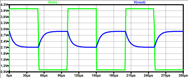
LTSpice:
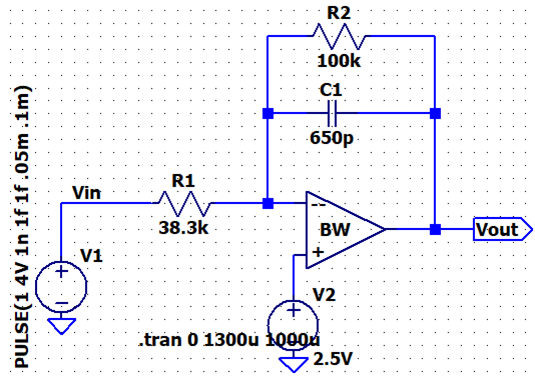
Output:
From LTSpice, we can see that we get our hand-calculated ΔVout from 1V to 4V or change of 3 Volts at the
output.
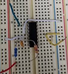
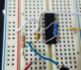
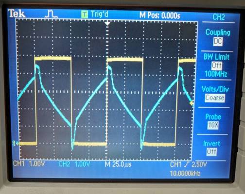
Lets build it!
BreadBoard:
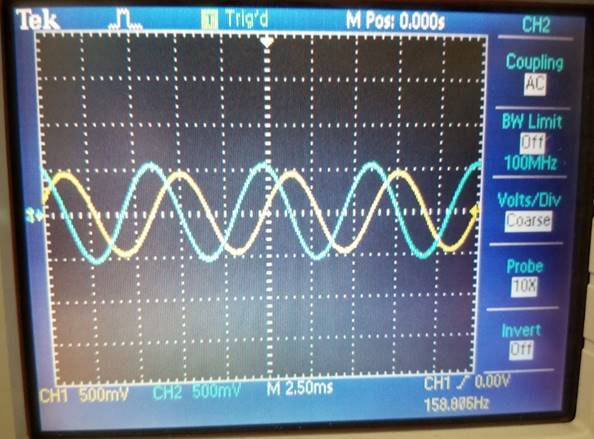
Oscilloscope
output:
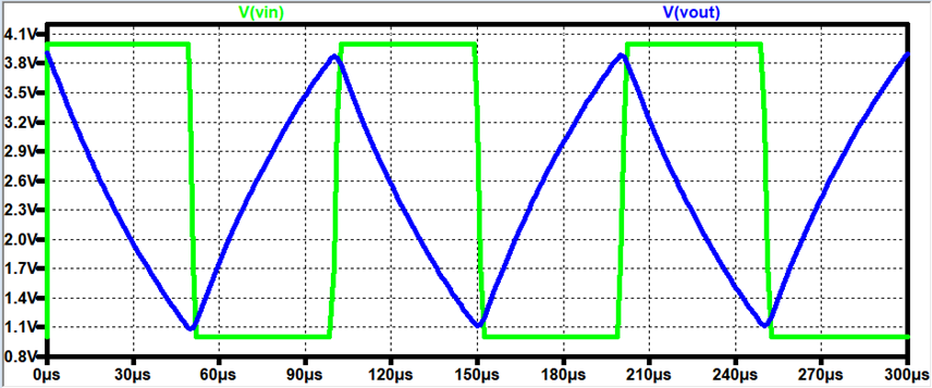
Experimentally,
our Output looks a lot like our LTSpice output and
goes from 1V to 4V (I chose a Vin of 3Vpp so that it would be easier to see our
output match our input).
We do have
that small error in our bottom Vout, and that could
be due to our Output swinging way near Vcc- due to
the VOffset (or GND).
So, lets go
back to what happens with RBig, if suppose it was too
small because we want to get rid of that nasty little Voffset:
Rbig =
10kΩ
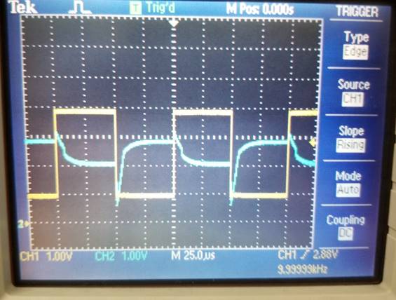
LTSpice:
As students,
we would say “What the H, Man?? Circuits broken”, but from a logical point of
view, if Rbig gets too small, lets
say to 0Ω, then our Vcm will short to Vout, meaning that our output will get closer to Vcm with smaller Rbig.
So what if we use a big Rbig, lets say 200kΩ?
Vout = 10mV (1
+ 200/38) = 63mV, 2.5+.063 = 2.56 V, will affect it a bit more
LTSpice: Note: Max Vcc+
is 5V, Wish I could make an Op-Amp with this, it should clip to ~5V
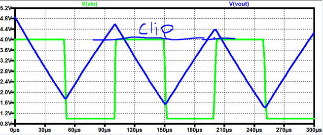
We will see
that nasty little VOffset bug our output,
making the output almost want to rail to GND and 5V.
There are
trade-offs when it comes to wanting the right signals at the output. If we
wanted a smaller input signal, we will be using a smaller Ri, but that would
make our circuit sensitive because Ri needs to be big enough so that we don’t
see the Offset voltage.
If we wanted
to use a big capacitor, we will also be seeing a super small resistance, which
means that little Offset voltage will give us a sad output.
Overall, our
Offset Voltage, and our limitations of Vcc+/- will
affect what we really want at the output. If we used bigger limitations such as
a higher Vcc+, we can have more workspace for our
output swing.