Lab 3 – OP Amps I
EE 420L Analog IC Design
Lab Date: 2/06/19 Due: 2/20/19
Last Edited on 2/19/19 at 9:45pm using Word
In this lab, we will be going over how Operational Amplifiers (Op
Amps) work to make small signals become amplified.
Suppose we have a small signal such as a pulse or a sound and we
would want to see it happen at a large scale. The Op Amp is here to help us see
what the small signal looks like. The Op amp has a few important terminals; A
VCC+ and VCC- to make sure that the Op amp is “powered,” two inputs that are
connected to a very high impedance, and an output, which is equaled to the
difference of the inputs multiplied by a very LARGE Open-Loop Gain (or AoL).
--------------------------------------------------------
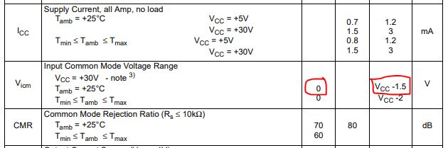
Datasheet and Review:
- Knowing
the non-inverting input, Vp, is at the same potential
as the inverting input, Vm, (called the
common-mode voltage, VCM) what are the maximum and minimum allowable
common-mode voltages?
- Support
your answer with an entry from the electrical characteristics table in
the datasheet.
-Given that VCC+ = +5 Volts and VCC- = 0 Volts;
T
The Maximum
allowable VCM Voltage is: VCC
– 1.5V given that the Op amp is operating at T = 25˚C.
~So for our circuit, our max VCM will be 3.5V. We
will choose to operate at VCM = 2.5V, so that we have an equal
amplitude distance from VCC+ and VCC-
The Minimum
allowable VCM Voltage is: 0V
given that the Op amp is operating at T = 25˚C.
~So for our circuit, We will not be utilizing 0V because we
will be using only ONE power supply.
The only reason why we could use VCM
= 0V is if we use 2 Power Supplies and use VCC+ = 15V and VCC- = -15V so that we can have a LARGER Voltage swing but the
drawback is that we will be using a dual
power supply setup.
- This can all be seen within the LM324.pdf
datasheet, here is a snippet below:
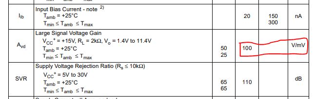
- What is a good estimate for the op-amp's open-loop
gain?
- Support your answer with a plot from the datasheet and
an entry from the electrical characteristics table.
-A good estimate for a
good Op Amp is usually AoL = 1MEG (106)
V/V gain. For this Op Amp, the Open-Loop Gain is given by AVD
(A.K.A. AoL) = 100 V/mV (or 105 V/V) gain.
~We want a higher Open-Loop Gain because we want to assume that
theoretically Vp=Vm or:
Vout
----- = AoL And
with the assumption, we will have a high Open-Loop Gain.
(Vp
– Vm)
Here is a snip from the datasheet
- What is a good estimate for the offset voltage?
- For worst case design what value would you use?
-A good
estimate for the offset voltage is usually 10mV offset, so that depending on
our actual Op-Amp gain (Let’s assume Vout/Vin Gain =
100), we will have a Vout offset of around ±1V.
-In the
worse case scenario (Lets
say Voffset = 100mV), we would use a Vout/Vin gain of 5 or less, so that our Vout
offset will be around ±500mV. It is a bad output, but if we used a larger gain,
we will be amplifying the offset by a lot more. We generally want to use lower
Gains to lower the effects of the offset voltage.
----------------------------------------------------------------------------------------------------
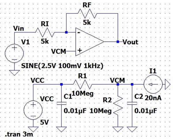
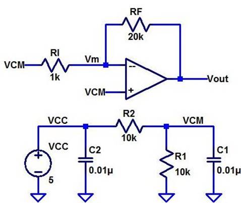
Experiment 1: (Building an
inverting Op-Amp Circuit)
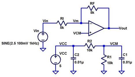
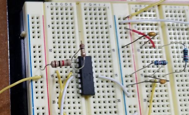
Breadboard:
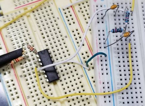
NOTE :All resistors are
relatively near their respective values and precision is not important. We will
be observing the basics of the Op-Amp and how to set it up under different
scenarios.
Output:
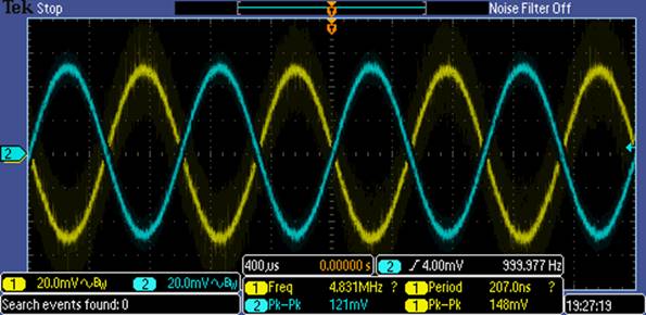
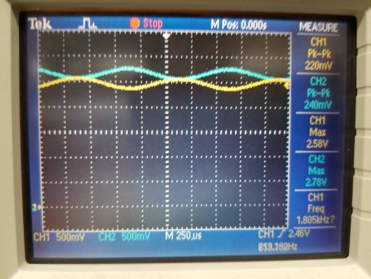
Vin = 148mV, Vout = -121mV, Gain = Vout/Vin = -0.818 V/V
LTSpice Output:
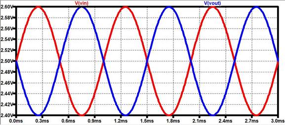
Vin = 100mV, Vout = 100mV, Gain = -1 V/V
- What is the common-mode voltage, VCM? Does VCM change?
Why or why not?
-In this
Circuit, VCM = 2.5V, VCM does not change since it is a DC
voltage. The decoupling capacitors are there to make sure we do not have any
small variations of Voltage throughout our power circuit (The circuit providing
the VCM).
- What is the ideal closed-loop gain?
The
ideal closed-loop gain should theoretically be our Gain = -Rf/RI, so whatever
resistor we place into our circuit would be theoretically seen by our gain
factor. So if we use RF=RI=5k, then we theoretically
should be getting Gain = -1 V/V
- What is the output swing and what is it centered
around?
-The
output swing for this circuit is about -121mV swing, and it swings around 2.5
Volts.
- What happens if the input isn't centered around around VCM, that is, 2.5 V?
If we
are not centered around 2.5 Volts, we will get clipping if our output swing
goes above VCC+ = +5V or if our output swing goes below VCC- = 0V.
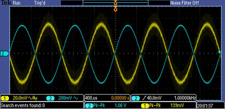
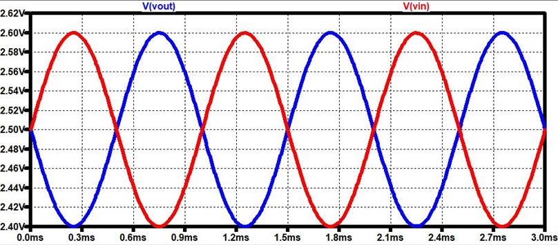
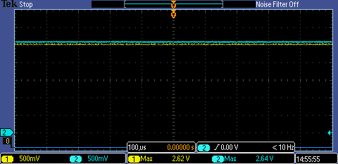
~IF we increased the amplitude from 100mV to about
2.5-2.6Vpp, we will theoretically have a
2.5-2.6Vpp output swing. Below is what the Op-Amp
outputs with these kinds of conditions:
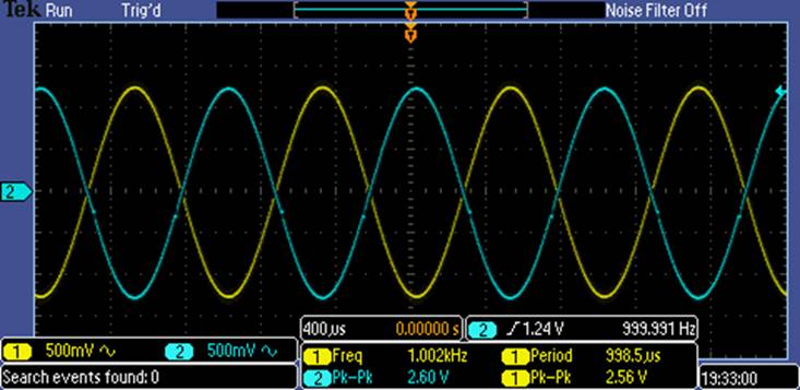
From the picture, we can see that we are still at
a Vout/Vin Gain of -1 V/V.
HOWEVER… If we
increased the input voltage to something higher such as 3Vpp, we will get clipping, as seen below:
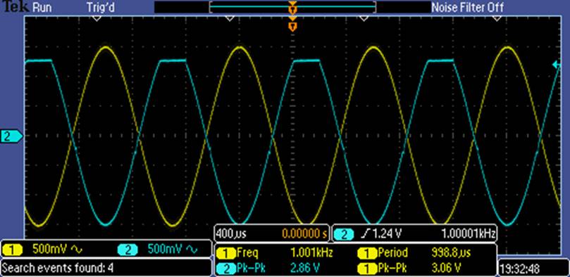
This
clipping occurs because we are going “Outside” the acceptable barriers of the
Op-Amp. The VCC+ and VCC- of the Op-Amp act like a barrier or some kind of
Max/Min output that can occur from the Output Swing.
Once the
Output Swing is Greater than or equal to
2.5V(VCM) +2.5 Output Voltage Swing, our voltage then “clips” to the
maximum value of 5 volts VCC+. This also can occur with the bottom, as if the
Output Swing is Less than or equal to
2.5V(VCM) – 2.5 Output Swing, the bottom clips to the minimum value
of 0 volts VCC-.
Below is
another example of if our VCM is lower than 2.5V and is clipping
downward:
- What is the maximum allowable input signal amplitude?
Why?
-Just as
stated above, the Maximum Allowable Input Signal Amplitude is 2.5Vpp because if we
It is
2.5V since if we go above 5V (Our VCM plus 2.5V Swing), we start to clip to
both the top and the bottom of the VCC barriers.
- What is the maximum allowable input signal if the
magnitude of the gain is increased to 10? Why?
-Since
we are multiplying our input by a Gain of 10, we should choose a gain that will
not go pass the VCC barriers of 0V and +5V. For this circuit, the Maximum Allowable input signal is 0.25Vpp, so that our output swing will
be theoretically 2.5Vpp. Passing the VCC barrier would then result in the
clipping scenario as seen above.
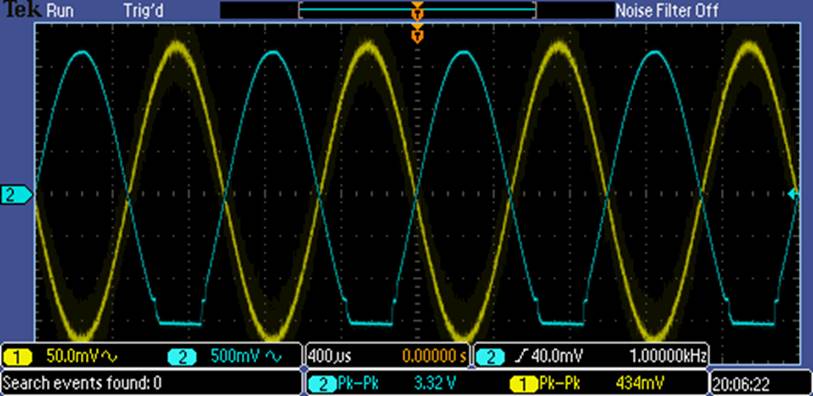
Here
below is our Gain of 10 V/V:

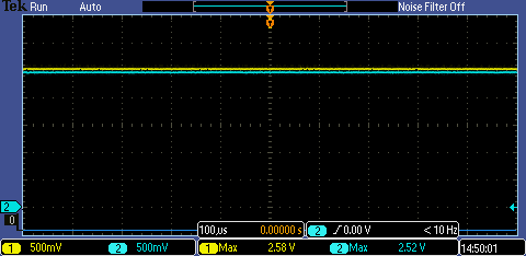
Vin =
~100mV, Vout = 1.06V
Here is
a pic of our output swing being clipped if we increase the input voltage:
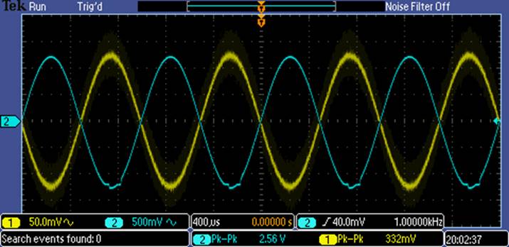
Vin =
332mV, Vout = ~2.56V
With the
new higher gain, small input voltages will impact our output a lot more.
- What is the point of the 0.01 uF
capacitors from VCC and VCM to ground?
-The
0.01 uF capacitors in our power circuit are called Decoupling capacitors and are used to
“clean up” the DC voltage from any small frequencies and to keep a constant
clean DC current. The capacitor basically shunts any nasty noise that we don’t
want in our Op-amp Circuit and will keep our circuit nice and happy.
A Great analogy for the Decoupling
capacitor is to imagine the capacitor as a “Storage Containter”
of water. If we have a river of water powering a Windmill, we want constant
flow. Knowing that rivers are wild and random, there won’t be constant current
throughout the river. To solve this, a “Container” is placed very close the Windmill so that we can
always have a constant flow of water.
It is
important to have decoupling capacitors so that noise is removed from any
outside interference. It is also good practice to have them in your PCB
designs. Here’s a pic for you :-)

- Are these values critical or could 0.1 uF, 1,000 pF, 1 uF, etc.
capacitors be used?
If we
use bigger capacitors, going back to our water container analogy, it would help
out with some of the “bigger waves of water” or a high variation in frequency,
however, at the cost of having more expensive pieces for your PCB. A small capacitor
is used to clean up those very fast frequencies and ripples that are in the
current.
- The data sheet shows that this op-amp has an input bias
current that flows out of the op-amp's inputs of typically 20 nA.
- The current flows out of both the non-inverting and
inverting inputs through the resistors connected to these inputs.
- Show how the operation of the circuit can be affected
if, for example, R1 and R2, are much larger. Explain what is going on.
- What is the input offset current? What does this term
describe?
-During
all of our procedures, we have neglected a small input offset current that is
coming out from the Op-Amp’s terminals. Here is what we are actually testing:
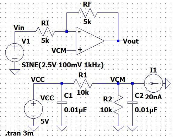
However,
the current does little to no effect to our circuit, since the 20nA current
through R2 of 10k will give us an added voltage drop of .2mV, which will not affect
VCM at all (So VCM = 2.502V, which just rounds to 2.5V).
Experiment:
LTSPICE:
^Circuit
doesn’t really change at all:
Suppose R1
= R2 = 10MEG, as seen below:
Now this
is where things go crazy. Obviously by the Voltage divider, VCM =
2.5V,
HOWEVER… The 20nA offset current
going through R2 will make an effect on our circuit by adding some unwanted
voltage to our VCM circuit.
The new
voltage drop will be V = 20nA(10MEG) = 0.2V, so our new VCM =
2.5+0.2 = 2.7V!
Now the
voltage at the non-inverting and inverting terminals will be at a higher voltage (So higher VCM
means Output Swing Offset will go up too), meaning that now the current through
the Op-Amp circuit will and affect Vout, in which Vout’s DC Offset will be Greater Than Vin’s DC Offset, assuming that the Gain = 1 V/V.
Experiment:
NOTE: As you can see, Vout (Blue) is shifted
up by about 0.2V, and the extra voltage is because of the small extra current
that is running out from the Op-Amp into VCM.
LTSPICE: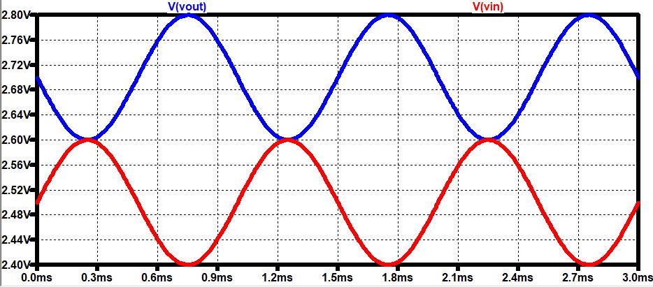
LTSpice also proves this too.
--------------------------------------------------------------------------------------------------------
Experiment 2: (Measuring
the Offset Voltage)
- Note that if the output voltage is precisely the same
as VCM then the op-amp has no offset voltage (this is very possible).
- To measure small offset voltages
increase the gain by increasing RF to 100k or larger. Explain what is
going on.
- Measure the offset voltage of 4 different op-amps and
compare them.
To measure the Offset
Voltage, we will need to disconnect our Input sine voltage and replace it with our
VCM voltage. Theoretically we can imagine VCM as our “Reference Ground” and
assume that there is little to no current running through our circuit, so the
only Theoretical voltage we should be seeing is the Offset voltage that is
coming from the Non-Inverting Terminal. It works the same as any other circuit,
calculate Vout and dividing it by your Gain, however,
Vout in this case will be our Offset voltage that we
want to find. To find it, we will be using a high gain of about 100k, and then
dividing our DC voltage difference by a gain of 100 V/V.
Breadboard:
First Op-Amp:
VDifference = 20mV
After changing
the RF = 100k, we got to see the differences between the input VCM
and Vout, and the multiplier for this circuit is 100
V/V.
To Calculate
this Offset, we get our VDifference and divide it by
our Gain, which is 100 V/V, so for this first Op-Amp, our offset will be 0.2mV
Second Op-Amp:
VDifference = 60mV
Our offset
will be .6mV

VDifference = 160mV
Offset = 1.6mV
Fourth Op-Amp:

VDifference = 120mV
Offset = 1.2mV
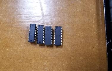
Chips tested: 4
Different LM324 Op-Amp Chips
Looking at all
of the Op-Amp’s :
|
1st |
2nd |
3rd |
4th |
|
.2mV |
.6mV |
1.6mV |
1.2mV |
We can see
that they are all not the same, even when they are from the same family of Op-Amps.
The reason for this is that Manufacturing is not always perfect, and also the month
and year each individual chip was made. For 2 chips to be identical, you’d have
to make them both at the same time.