EE 420L
Engineering Electronics II Lab
Lab 6 - Single–stage
transistor amplifiers
email: matacarl@unlv.nevada.edu
3/27/19
Pre-lab:
- Review
these datasheets and become familiar with these transistors.
- Verify
that the simulations seen in lab6_sims.zip reasonably
model the behavior of the transistors' ID v. VGS, ID v. VDS, and gm v. VGS
curves.
- Finally,
watch the video single_stage_amps and
review single_stage_amps.pdf
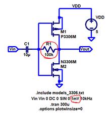
Lab description:
The goal of this lab is to understand basic MOSFET amplifier
topologies, such as Common-drain amplifier (Source follower), Common-Source
amplifier, Common-gate amplifier, and Push-pull amplifier. Find input and
output resistances, currents, voltages, and gains.
This lab will utilize
the ZVN3306A and ZVP3306A MOSFETs.
How to measure the input resistance?
A resistor equal to the theoretical input resistance
(50k||100k) is added in series with the input voltage; the new resistor should
be between the input Vin and the capacitor C1. By doing this the gate voltage
should be half the input when simulated. If the gate voltage is not half, then
this gate voltage value can be used to calculate a resistor that would give a
new gate voltage that is half the input voltage. Taking the voltage difference
between the input voltage and gate voltage, and dividing that difference by the
resistor, gives the input current. Now, dividing the gate voltage by the input
current gives the input resistance.
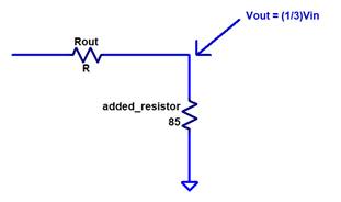
How to measure the output resistance?
A resistor equal to the theoretical output resistance is
added between the output and VDD or ground, depending if it’s NMOS based or
PMOS based. By doing this the output voltage should be half the input voltage.
If the output voltage is not half, then this voltage value can be used to
calculate a new resistor value that would produce an output voltage equal to
half the input. Dividing the output voltage by the added resistor gives the
output AC peak current. Then taking the difference in voltage between the input
and output and dividing that by the peak output current, provides us with the
output resistance.
|
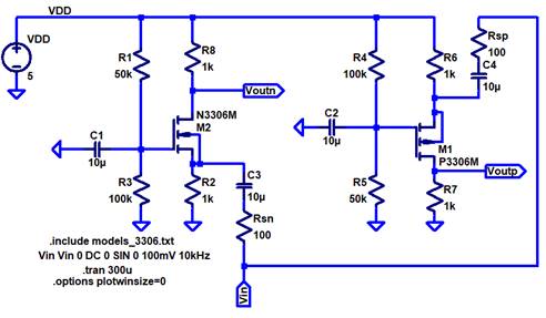
Common-Drain Amplifier (source follower), NMOS and PMOS |
|
|
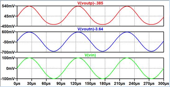
Operation of this circuit: For this amplifier
the output voltage is almost the same value as the input voltage. Thus, this
has a gain of one, which is the reason is call a source follower. This
topology is used as a voltage buffer because the output current is much
higher than the input current. The NMOS SF produces an output current that is
1 thousand higher than the input current. The PMOS SF produces an output
current that is over 130 times higher than the input current. The DC voltage of
the circuit is the output of a voltage divider, which is being used to biased the NMOS and PMOS. The DC current can be calculated
using the gate voltage and applying KCL to the circuit. |
|
|
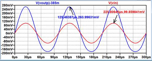
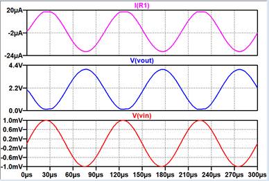
LtSpice simulations for original circuit, no added impedance
|
|
|
Hand
calculations NMOS
Gain
|
Hand
calculations PMOS
Gain
|
|
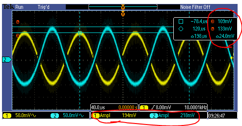
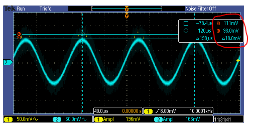
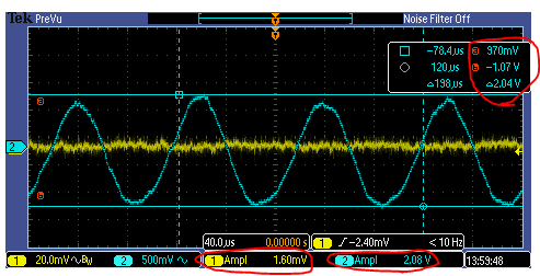
Experimental
results using NMOS, original circuit, no added impedance
|
Experimental
results using PMOS, original circuit, no added impedance
|
|
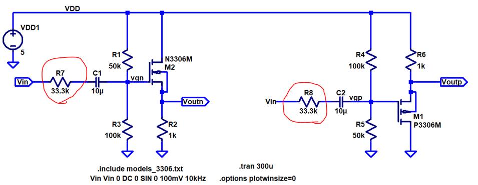
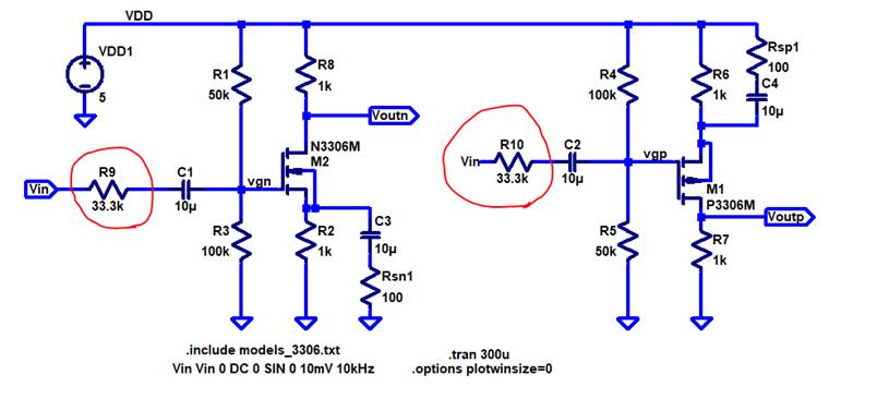
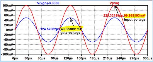
Schematic with added resistors
equal to Rin=33.3k
|
|
|
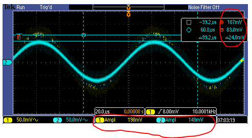
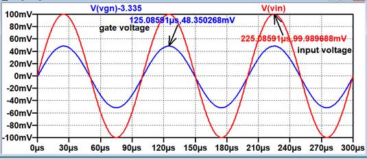
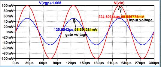
simulations plot
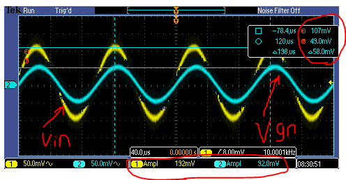
with resistor equal to Rin=33.3k to find input resistance for NMOS side
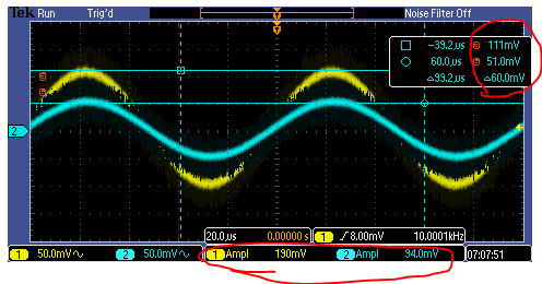
Experimental
result Used resistor =
32.3kΩ
|
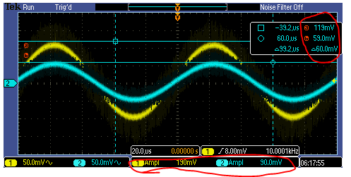
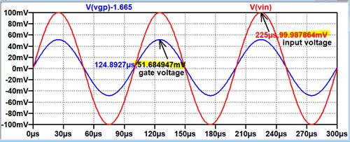
simulation plot
with resistor equal to Rin=33.3k to find input resistance for PMOS side
Experimental
result Used resistor =
32.3kΩ
|
|
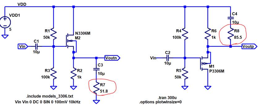
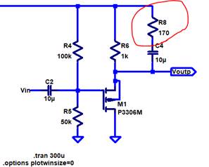
Schematic with added impedance
equal to Rout=51.8Ω
|
|
|
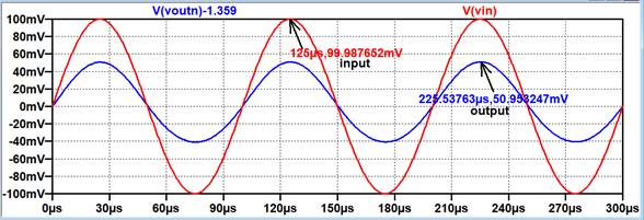
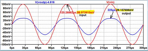
simulations plot
with impedance equal to Rout = 51.8Ω to find the output resistance for
NMOS side
Resistor value
used was 50.56Ω
|
simulations plot
with impedance equal to Rout = 85.01Ω to find the output resistance for
PMOS side
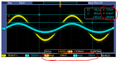
Experimental
results NOTE: Our simulations
on the oscilloscope gave us 1/3 of the input voltage, using 85Ω. However,
by using this output voltage, 1/gm for pmos was
solved.
This new Rout
was used for our new plot and experimental set up
|
|
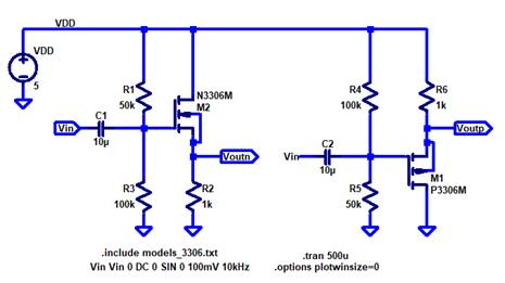
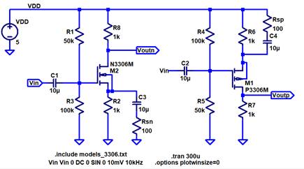
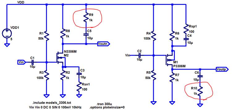
Common-Source Amplifier, NMOS and PMOS |
|
|
Operation of this circuit: For this circuit
the Source terminal is common to the input and output. The gain for this
circuit is the resistance in the drain divided by the resistance in the
source. And because the resistance in the source is smaller than the output
resistance, there is a gain depending on how small the value of Rs is. The
lower the value of Rs, the higher the gain. Also, because the gain goes up,
the output current drops lower than the output current for the Source
follower. The DC voltage of
the circuit is the output of a voltage divider, which is being used to biased the NMOS and PMOS. The DC current can be calculated
using the gate voltage and applying KCL to the circuit. |
|
|
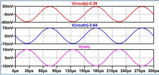
LtSpice simulations for original circuit, no added impedance
|
|
|
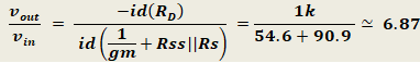
Hand
calculations NMOS
Gain
|
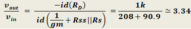
Hand
calculations PMOS
Gain:
|
|
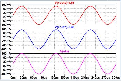
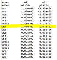
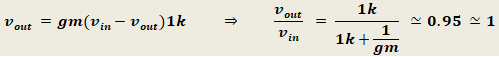
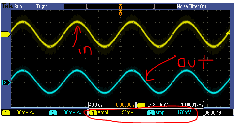
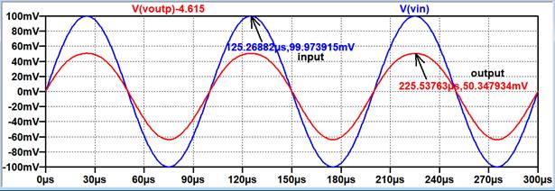
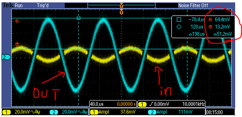
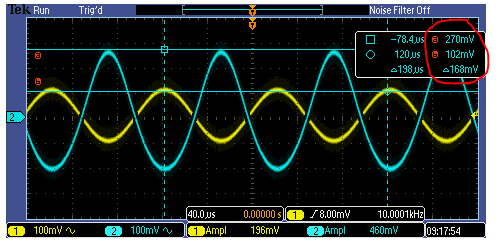
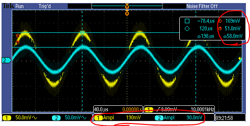
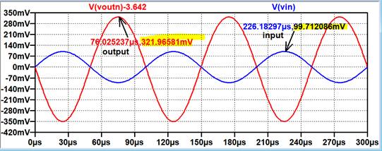
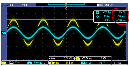
Experimental
results using NMOS, original circuit, no added impedance
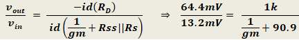
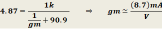
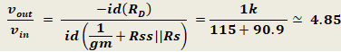
NOTE: We can see from
the result above that the gain is about 4.87 and not as was calculated in the
hand calculations, which says that the gain is about 6.87. So, we used this
output value and solve for the gm of the NMOS.
Thus, Gain
|
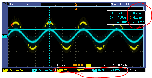
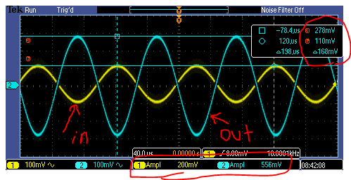
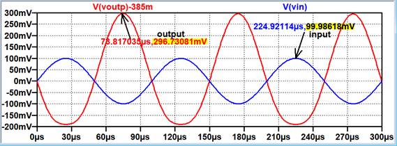
Experimental
results using PMOS, original circuit, no added impedance
The gain is a
little lower than we calculated. About 2.65 |
|
Schematic with
added resistors equal to Rin=33.3k
|
|
|
simulations plot
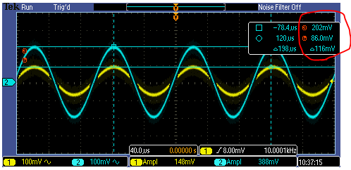
with resistor equal to Rin=33.3k to find input resistance for NMOS side
Experimental
result: Used resistor =
32.3kΩ Used 200mVpp as
Vin, 100mVp
|
simulation plot
with resistor equal to Rin=33.3k to find input resistance for PMOS side
Experimental
result Used resistor =
32.3kΩ Used 200mVpp as
Vin, 100mVp
|
|
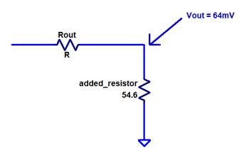
Schematic with
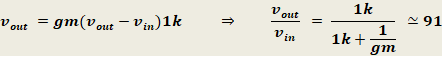
added impedance equal to Rout=1kΩ
|
|
|
simulations plot
with impedance equal to Rout = 1kΩ to find the output resistance for
NMOS side
Experimental
results Resistor value
used was 1kΩ
Gain is about 2.5,
which is expected because we calculate the gm of the NMOS experimentally.
This new gm gave us a gain of about 4.85. Thus, the output voltage should
have a gain of about 2.5
|
simulations plot
with impedance equal to Rout = 1kΩ to find the output resistance for
PMOS side
Experimental
results Resistor value
used was 1kΩ
The output gain
is about 1.22, which is about half of the gain calculated experimentally,
2.65
|

|
Common-Gate Amplifier, NMOS and PMOS |
|
|
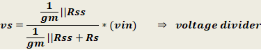
Operation of this circuit: The gain for
this circuit is basically the output resistance divided by the addition of
1/gm and Rsn. Again
because the addition of 1/gm and Rsn are smaller
than the output current, there is a gain depending on the value of Rsn. The smaller the value of Rsn,
the higher the gain, but the current get smaller as well. The DC voltage of
the circuit is the output of a voltage divider, which is being used to biased the NMOS and PMOS. The DC current can be calculated
using the gate voltage and applying KCL to the circuit. |
|
|
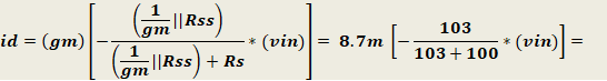
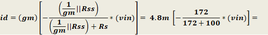
LtSpice simulations for original circuit, no added impedance |
|
|
Hand
calculations NMOS
Gain
|
Hand
calculations PMOS
Gain
|
|
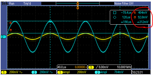
Experimental
results using NMOS, original circuit, no added impedance
The gain is about
4.3, which is close to what was calculated above. |
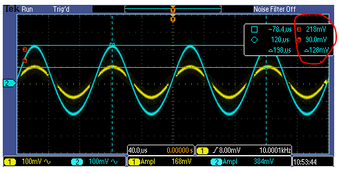
Experimental
results using PMOS, original circuit, no added impedance
The gain is a
little lower than we calculated. About 2.4 |
|
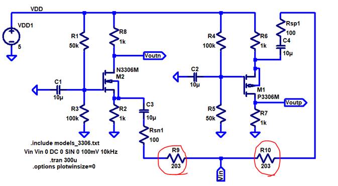
Schematic with
added resistors equal to Rin=203Ω
|
|
|
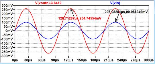
simulations plot
with resistor equal to Rin=203Ω to find input resistance for NMOS side
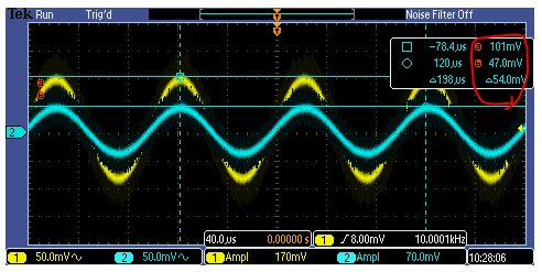
Experimental
result: Used resistor = 198Ω Used 200mVpp as
Vin, 100mVp
|
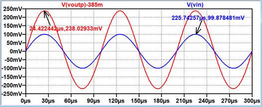
simulation plot
with resistor equal to RinΩ=203 to find input resistance for PMOS side
Experimental
result Used resistor = 198Ω Used 200mVpp as
Vin, 100mVp
|
|
Schematic with
added impedance equal to Rout=1kΩ
|
|
|
simulations plot
with impedance equal to Rout = 1kΩ to find the output resistance for
NMOS side
Experimental
results Resistor value
used was 1kΩ
Gain is about 2.3,
close to half of the original gain calculated in the hand calculations
section
|
simulations plot
with impedance equal to Rout = 1kΩ to find the output resistance for
PMOS side
Experimental
results Resistor value
used was 1kΩ
The output gain
is less than 1, which is less than half of the 2.4 gain calculated
experimentally
|
|
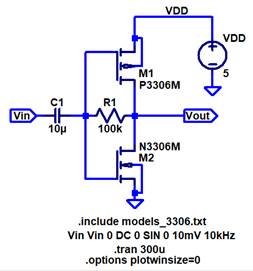
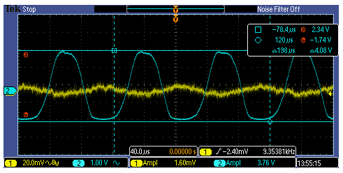
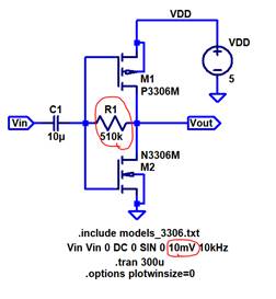
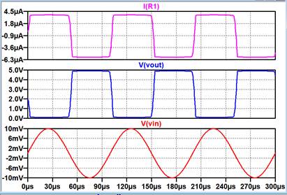
Push-Pull Amplifier |
|
|
Operation of this circuit: This amplifier has
a topology like an inverter in which the output can swing from VDD to ground.
As AC input current swings, the output swings close to the rails. The AC
input current causes the NMOS or PMOS to turn on and shut off, which is the
reason the output can swing up to the VDD and ground, and this is also the
reason for such a big gain. For the DC part
of the circuit, both NMOS and PMOS are diode connected, which means they are
in saturation, and current is flowing through both |
|
|
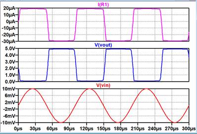
LtSpice simulation |
|
|
Hand calculations
Gain:
The output is -13.5V,
but since 5V is the maximum voltage it can reach, it clips at 5V and the wave
looks like a square wave |
|
|
LtSpice simulation with 100k resistor and 1mVp
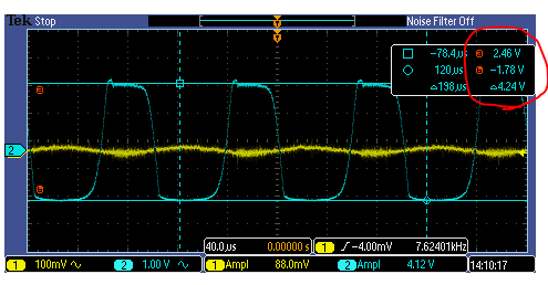
Experimental
result:
|
LtSpice simulation with 510k resistor and 100mVp
Experimental
result:
|
Return to student lab reports
Return to labs