EE 420L Engineering Electronics II - LAB 9
Authored by
David Flores
Email: flored6@unlv.nevada.edu
Due: April
24, 2019
Lab Description
Design of a Beta-Multiplier Reference (BMR) using the CD4007 CMOS
transistor array
Pre-lab
Pre-lab work
- This
lab will use the level=1 MOSFET model created in lab 8 and, again, the
MOSFETs in the CD4007.pdf CMOS
transistor array.
- Design
and simulate the operation of a BMR that biases the NMOS devices so that
they have a gm of 20 uA/V
- Use
a simple (big) resistor to VDD for the start-up circuit (explain how the
addition of a resistor ensures start-up).
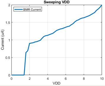
- When
the BMR is operating the current in the big resistor should be much
smaller than the current flowing in each branch of the BMR
- Write-up,
similar to a homework assignment, your design calculations and simulation
results. (This will count as the pre-lab quiz.)
- Ensure
that you show the following in what you turn in:
- Hand
calculations
- Operation
as VDD is swept from 0 to 10 V
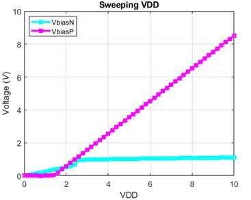
- Vbiasn should stabilize (be constant)
after VDD hits a minimum value (estimate this value of VDD assuming
VGS/VSG is a threshold voltage and VDS,sat/VSD,sat is zero).
- Vbiasp should follow VDD after VDD hits a
minimum value (show this in simulations)
- Unstable
operation if too much capacitance is shunting the BMR's resistor (see
bottom of page 630)
- Comments
comparing the hand calculations with the simulation results
Lab Instructions
In this lab you may need to use two,
or more, CD4007 chips from the same production lot (see date code on the top of
chip) to ensure using a BMR to bias a current mirror is possible. If the CD4007
chips are not from the same production lot they will not "match" so
current mirrors will not be possible.
- Build
your BMR design and characterize it as you did in the pre-lab
- You
expect the BMR to become unstable if there is a large capacitance across
the resistor, such as a scope probe (important), so care must be
exercised
- Use
your BMR to bias, and thus create, a:
- NMOS
current mirror
- PMOS
current mirror
- Measure
how the current varies through each current mirror as the voltage across
the mirror changes.
- Of
course the current in the NMOS (PMOS) current mirror goes to zero as the
voltage on the drain of the output device moves towards ground (VDD)
- Using
these current mirrors drive two gate-drain connected transistors
- For
the first experiment use the NMOS current mirror to drive two PMOS
gate-drain connected devices.
- Use
the voltages on the gate-drain connection of the two devices to bias a cascode current mirror (characterize this mirror as
before)
- For
the second experiment switch, that is, use the PMOS current mirror to
drive two NMOS gate-drain connected devices.
- Again,
use these two voltages to bias an NMOS cascode
current mirror then characterize.
Experiment
0: Prelab
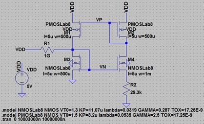
Ltspice schematic Beta Multiplier
Gm
equation to solve for ID:
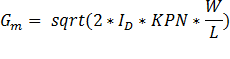
![]()
ID = 180.6nA
Solving
for the resistance R:
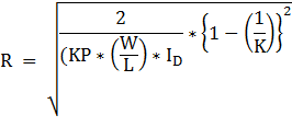
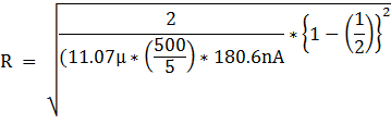
R = 29.3kΩ
For the prelab we chose a 1Gohm Resistor as our startup circuit
this is so that a small current can go through small enough to get the NMOS
gate going. This current cannot be to large or it will affect how the BMR operates.
Ltspice Schematic Results BMR
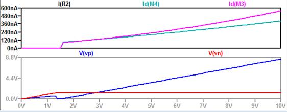
Experimental Results for NMOS and PMOS BMR here we swept VDD
from 0-10V with increments of 0.5V
Note: The
reason we did it in this order and not in the order instructed was because we
messed up our calculations and had to go back and fix our results. So we have Exp.1
NMOS current mirror followed by the NMOS current mirror with PMOS gate-drain
loads followed by the NMOS current mirror with PMOS Cascode
circuit. Then we will have the Exp.2 PMOS current mirror followed by the PMOS
current mirror with NMOS gate-drain loads followed by the PMOS current mirror with NMOS Cascode circuit.
Experiment
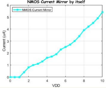
1: NMOS Current Mirrors
For this experiment we made an NMOS current mirror we used the
NMOS gate voltage from the BMR to bias the current mirror. We swept VDD from
0-10V with increments of 0.5V and plotted the graphs using MATLAB. We used an
IC chip seperate from the BMR but made sure to have
the same ground so that it wouldn't vary.
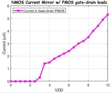
Here we will be using the NMOS current mirror this will drive
2 PMOS's Gate Drain connected we will be measuring the current the same way we
did previously.
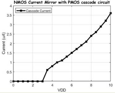
Finally we will built the Cascode
PMOS current mirror. We used the Gate Drain PMOS voltages
Here we can see all the graphs together in one plot
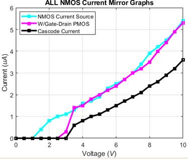
We can see that the blue and purple waveforms closely match
each other at least after about 3V I think that we actually had an error at 3V
and 2.5V which would match better.
Experiment
2: PMOS Current Mirrors
For this experiment we will be doing the same thing except
using the Complementary PMOS instead of the NMOS.

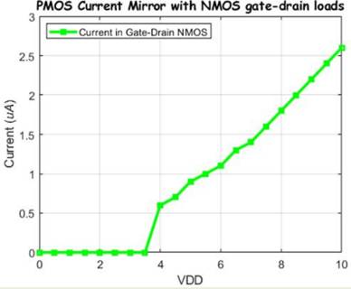
Here we will be using the PMOS current mirror this will drive
2 NMOS's Gate Drain connected we will be measuring the current the same way we
did previously.
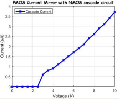
Here we will build the PMOS current mirror with NMOS cascode circuit
Here is all the graphs condensed into one plot
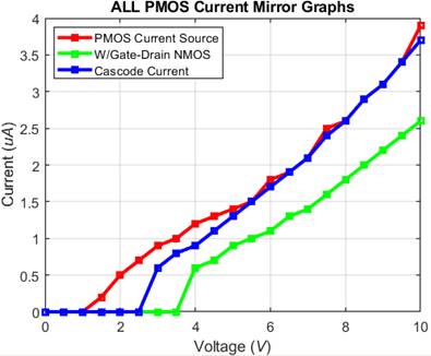
We can see that the NMOS cascode
current mirror matches the sourc current mirror with
Gate-Drain Connected NMOS loads.