EE 420L Engineering Electronics II - LAB 8
Authored by
David Flores
Email: flored6@unlv.nevada.edu
Due: April
10, 2019
Lab Description
Pre-lab
- Review
the datasheet for the CD4007.pdf CMOS
transistor array.
- Ensure
that you understand how the bodies of the NMOS are tied to pin 7 (VSS,
generally the lowest potential in the circuit, say ground) and that the
bodies of the PMOS are tied to pin 14 (VDD, generally the highest
potential in the circuit, say + 5V).
Lab Instructions
In this lab you will
characterize the transistors in the CD4007 (not the CD4007UB chip) and generate SPICE Level=1
models. Assume that the MOSFETs will be used in the design of circuits powered
by a single +5 V power supply. In other words, don't characterize the devices
at higher than +5 V voltages or lower than ground potential.
- Experimentally
generate, for the NMOS device, plots of:
1.
ID v. VGS (0 < VGS < 3 V) with VDS = 3 V
2.
ID v. VDS (0 < VDS < 5 V) for VGS varying from 1 to 5 V in 1
V steps, and
3.
ID v. VGS (0 < VGS < 5 V) with VDS = 5 V for VSB varying
from 0 to 3 V in 1 V steps.
- Note
that for this last one, if VSS (NMOS body) is ground (again, the
Body, VB, is grounded) then the source voltage will be varied from 0 to 3
V in 1 V steps to realize VSB ( = VS - VB = VS) varying from 0 to 3 V in 1
V steps. At the same time VGS will be varied from 0 to 3 V (when VS = 0),
1 to 4 V (when VS = 1 V), 2 to 5 V (when VS = 2 V), and 3 to 5 V
(when VS = 3 V). In other words, as VS is increased by 1 V the VGS has to
shift up by 1 V as well.
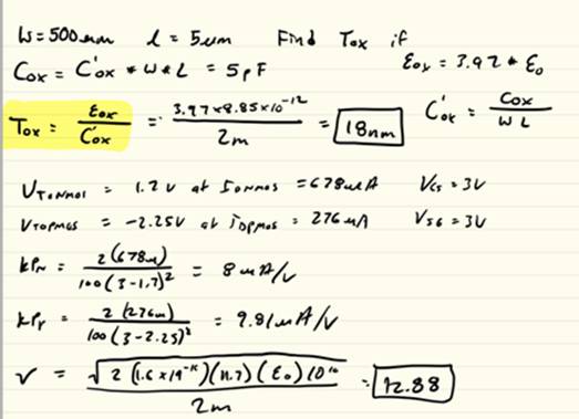
- Assuming
that the length of the NMOS is 5 um and its width is 500 um calculate
the oxide thickness if Cox (= C'ox*W*L) = 5 pF.
- From
this measured data create a Level = 1 MOSFET model with (only) parameters:
VTO, GAMMA, KP, LAMBDA, and TOX.
- Compare
the experimentally measured data above (the 3 plots) to LTspice-generated data (again, 3 plots) and adjust
your model accordingly to get better matching.
- Experimentally,
similar to what is seen on the datasheet (AC test circuits seen on page 3
of the datasheet), measure the delay of an inverter using these devices
(remember the loading of the scope probe is around 15 pF and there is
other stray capacitance, say another 10 pF).
- Using
your model simulate the delay of the inverter and compare to measured
results. Adjust your SPICE model to get better matching between the
experimental data and the measured data.
- Repeat
the above steps for the PMOS device where VDS, VGS, and VSB are replaced
with VSD, VSG, and VBS respectively.
Experiment
1: NMOS
For these experiments we used the UB chip in the instructions
it says not to use this chip but was later clarified by the professor that it
was okay to use them here is the layout.
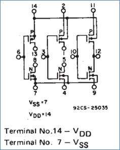
At first we used the leftmost NMOS consisting of pins 6,7,8
which were for gate, source and, drain respectfully. But we later realized that
for part 3 we needed to have a voltage difference between VS and VB so we used
the middle NMOS. This NMOS consists of pins 3,4,5 which were for gate, source
and, drain respectfully. This way we did not have the body of the NMOS and the
Source shorted so that we could have a different potential to see the effects.
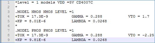
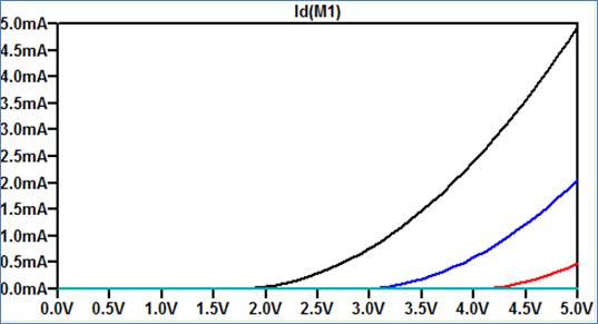
LTSpice Results will be presented
alongside the experimental results here is the LTSpice
MODEL
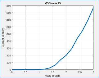
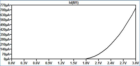
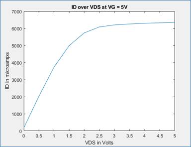
Part 1:
1.) ID v. VGS (0 < VGS < 3 V)
with VDS = 3 V
For this part we were going to graph ID vs. VGS with VDS
equaling to 3V and VGS being swept.
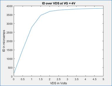
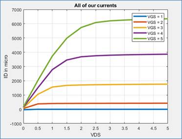
Part 2:
2.)
ID v. VDS (0 < VDS < 5 V) for VGS varying
from 1 to 5 V in 1 V steps, and
For this part we were to graph ID vs. VDS varying VDS from 0
to 5 and VGS varying from 1-5V (5 graphs).
VGS = 1V VGS
= 2V VGS = 3V
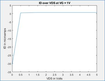
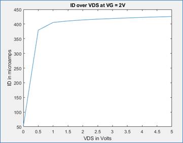
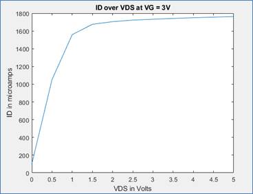
VGS = 4V
VGS = 5V
Here are all of the results compiled together on a single
graph.
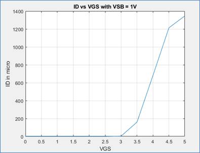
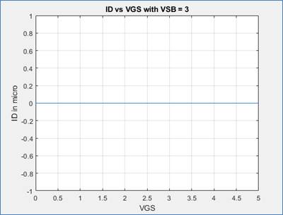
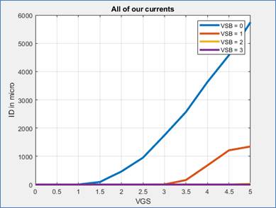
Part 3:
3.)
ID v. VGS (0 < VGS < 5 V) with VDS = 5 V for
VSB varying from 0 to 3 V in 1 V steps.
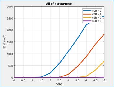
For this part we graphed ID vs. VGS with VDS at 5V
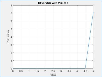
and VSB varying from 0-3V in 1V steps (4 graphs). Here VSB = 3V and VSB = 2V
are the same graph.
VSB = 0 VSB = 1V VSB =2V
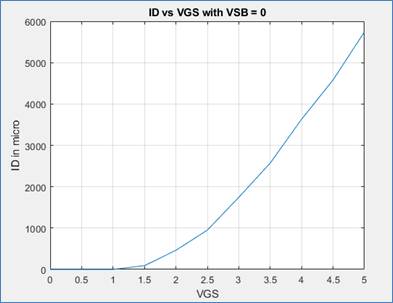
Here are all of the results compiled together on a single
graph.
Experiment 2: PMOS
For this experiment we used the top middle MOSFET
so we wouldn't run into the same problem as the previous experiment.
This PMOS consists of pins 3,2,1 which were for gate, source
and, drain respectfully. This way we did not have the body of the PMOS and the
Source shorted so that we could have a different potential to see the effects.
Part 1:
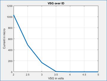
1.) ID v. VSG (0 < VSG < 3 V)
with VSD = 3 V
For this part we were going to graph ID vs. VSG with VSD
equaling to 3V and VSG being swept.
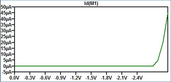
Part 2:
2.)
NOTE** As we keep going to
higher VSD voltages, our Battery source got to a point where it could no longer
have a higher VSG voltage. This could be due to the battery source sensing that
there is a “short” in the PMOS. Because of this we will have INACCURATE
measurements. For those higher VSD voltages at the higher constant VSG, we used
the same value as the highest max value of our VSG, so the lines will look
linear.
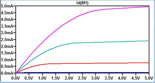
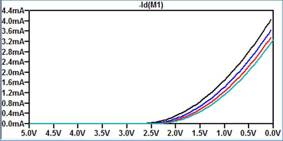
ID v. VDS (0 < VDS < 5 V) for VGS varying
from 1 to 5 V in 1 V steps, and
For this part we were to graph ID vs. VDS varying VDS from 0
to 5 and VGS varying from 1-5V (5 graphs).
VG = 4V VG
= 3V VG = 2V
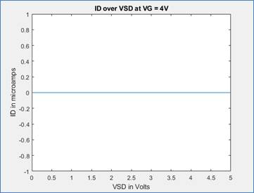
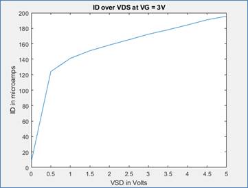
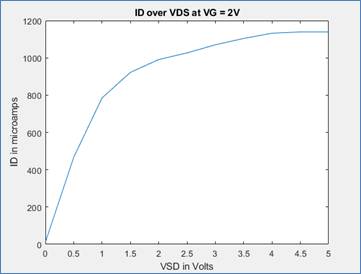
VG = 1V VG = 0V note* graph is labeled as VG = 1V it's actually 0V
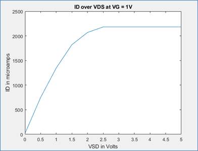
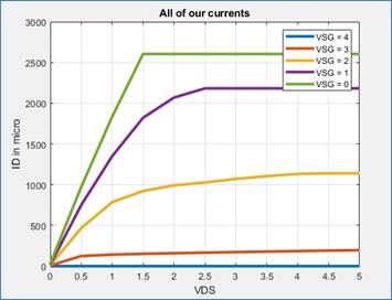
Here are all of the results compiled together on a single
graph.
Part 3:
3.)
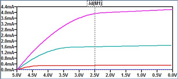
ID v. VSG (0 < VGS < 5 V) with VSD = 5 V for
VBS varying from 0 to 3 V in 1 V steps.
For this part we graphed ID vs. VSG with VSD at 5V
and VBS varying from 0-3V in 1V steps (4 graphs). Here VBS = 3V and VBS = 2V
are the same graph.
VBS = 0 VBS = 1V
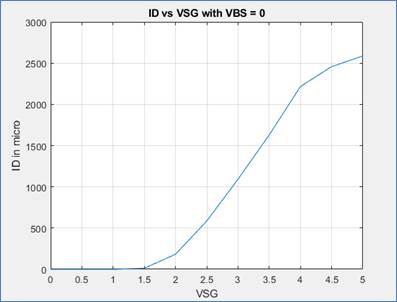
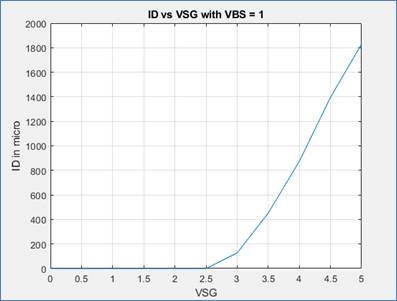
VBS =2V VBS = 3V
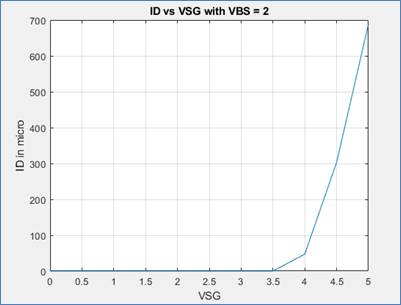
Here are all of the results compiled together on a single
graph.
Experiment
3: Hand Calculations
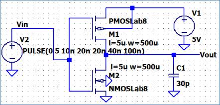
Experiment
4: The Inverter
In this experiment, we will
just be looking at how fast the Output reacts with the input of the inverter
and compare it with our LTSpice models. We will
have a small capacitance at the Probe tip, ideally 15pF, but there will be some
stray capacitance and we used 30pF to be safe.
Experimental Results
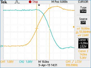
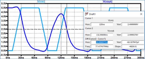
For the experimental we got 18ns delay and
for the LTSpice we got 13ns.