EE 420L
Engineering Electronics II - Lab 6
Authored
by David Flores
Email:
flored6@unlv.nevada.edu
Due:
March 27, 2019
Lab Description
In
this lab we will be using the the ZVN3306A and ZVP3306A MOSFETs. This lab will show how the Mosfets operate in a few different examples. The examples
consist of the Source Follower, Common Source Amplifier, Common Gate Amplifier,
and Push Pull Amplifiers.
Pre-lab
- This lab will utilize
the ZVN3306A and ZVP3306A MOSFETs.
- Review these
datasheets and become familiar with these transistors.
- Verify that the
simulations seen in lab6_sims.zip reasonably model the
behavior of the transistors' ID v. VGS, ID v. VDS, and gm v. VGS curves.
- Finally, watch the
video single_stage_amps and
review single_stage_amps.pdf
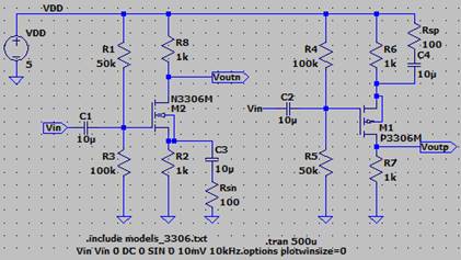
Experiment 1: Common Drain
Amplifier
Below are
schematics for NMOS and PMOS source followers amplifiers
(also known as common-drain amplifiers). In your lab report discuss the operation of these
circuits.
Common
Drain amplifiers also known as source followers, these circuits have a common
source with the gates of the mosfets acting as the
input and the drains of the mosfets acting as the
outputs. In some cases, the common drain amplifiers are used as a voltage
buffer. This will protect the input signal from the current drawn.
Hand
calculate, and then verify your hand calculations with experimentation
and simulations, the gains and the input and output
resistances ensuring that your test signals are at a high enough frequency
that the caps have negligible impedance but not so high that the gain is
dropping off.
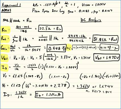
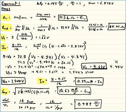
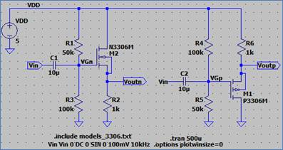
NMOS: PMOS:
Hand
Calculations: Hand
Calculations:
Simulate the
operation of these amplifiers.
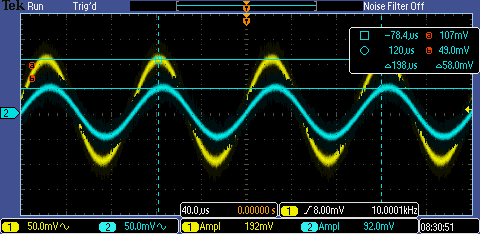
Spice Error Log .Op for Common Drain Circuit
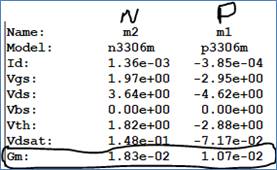
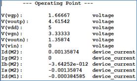
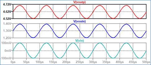
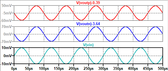
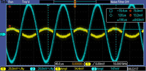
LtSpice Simulations for both NMOS and PMOS Ltspice waveforms for Voutp, Voutn and Vin
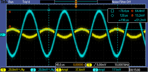
Experimental
Results:
VoutN: VoutP:
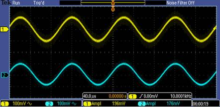
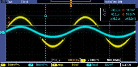
We
can see that the gain is close to 1 for both Mosfets
which matches the hand calculations above.
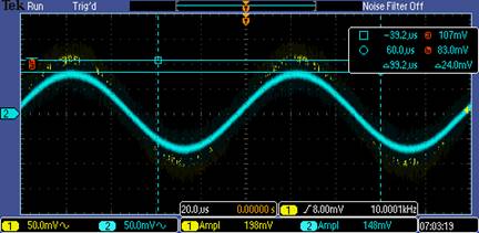
Nmos Input Resistance Pmos Input
Resistance
Nmos Output Resistance Pmos Output Resistance
If you build this circuit using electrolitic
capacitors, assuming the input AC signal swings around ground, put the
"+" terminal of the cap on the gate of the MOSFET. Please indicate,
in your lab report, that you understand why the capacitor is connected this way.
We
built the circuits with electrolytic capacitors the reason for the orientation is
because these capacitors are polarized which means that if we apply a negative voltage
on the wrong side we could destroy the capacitor causing it to pop.
Measuring Input Resistance
For
measuring the input resistance add a resistor equal to the value you calculated
between the input voltage source and the amplifier. We added this resistor and
then measured the voltages on both sides of the resistor to find the voltage
drop and calculate the current through the resistor To
find the input Resistance we finally we divide Vout
by this current through the resistor to get our input Resistance
Measuring Output Resistance
For
measuring output resistance, we added a resistor equal to the one calculated
from the output to ground. We can then measure the output resistance using the
voltage divider.
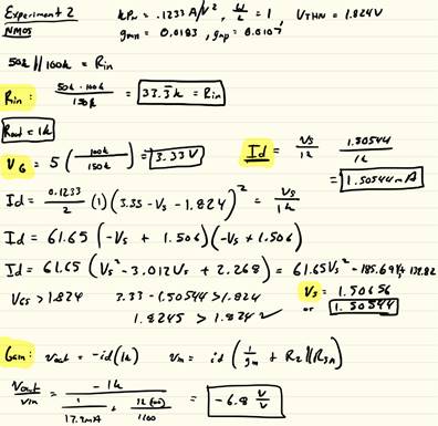
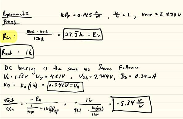
Experiment 2: Common Source
Amplifier
Hand calculate
the gains and the input/output resistances. How does the source resistance, Rsn or Rsp, influence the gain?
Again, compare your hand calculations
to simulation and experimental results.
NMOS: PMOS:
Hand
Calculations: Hand Calculations:
Simulate the
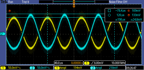
operation of these amplifiers.
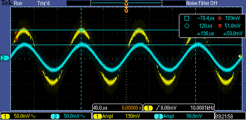
LtSpice Simulations for both NMOS and PMOS Ltspice waveforms for Voutp,
Voutn and Vin
Experimental
Results:
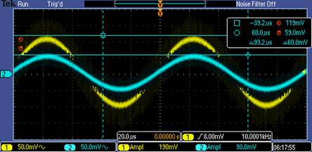
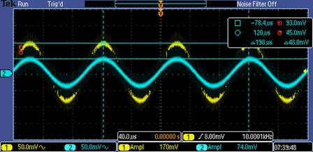
VoutN: Input Resistance 33k VoutP: Gain of 2.7
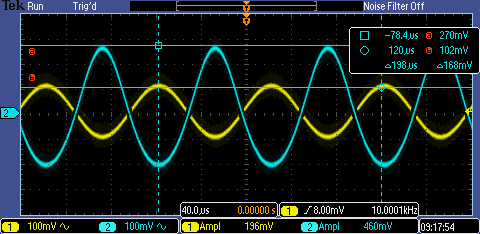
Changed Rsn to 50ohms 28.4k
Input Resistance
Gain
increases when Rsn decreases originally Rsn was about 100ohms gain was about 4.5V/V. Then we
changed Rsn to 50ohms and gain was about 6 (NMOS)
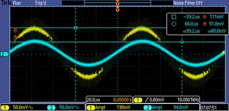
Added 32.3k resistor (input
voltage divider) Gain
of 1.3 Output Voltage Divider Rout is 1k