EE 420L
Engineering Electronics II - Lab 3
Authored
by David Flores
Email:
flored6@unlv.nevada.edu
Due:
February 20, 2019
Lab Description
In
this lab we worked with op-amps specifically the LM324 chip. We learned how to
read the data sheets to get important information, as well as all the
components that affect an op-amp. The following lab is done at Vcc+ = 5V and Vcc- = 0V.
Pre-lab
- Watch the video op_amps_I,
review op_amps_I.pdf (associated notes),
and simulate the circuits in op_amps_I.zip.
- Read
the write-up seen below before coming to lab.
Lab Instructions
This lab will utilize the LM324 op-amp
(LM324.pdf).
Review
the data sheet for this op-amp.
For
the following questions and experiments assume VCC+ = +5V and VCC- = 0V.
- Knowing the
non-inverting input, Vp, is at the same
potential as the inverting input, Vm, (called
the common-mode voltage, VCM) what are the maximum and minimum allowable
common-mode voltages?
- Support your answer
with an entry from the electrical characteristics table in the datasheet.
- What is a good
estimate for the op-amp's open-loop gain?
- Support your answer
with a plot from the datasheet and an entry from the electrical
characteristics table.
- What is a good
estimate for the offset voltage?
- For worst case
design what value would you use?
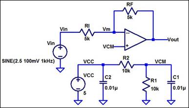
Build, and test, the following circuit. Note that a precise value for the 5k
resistors isn't important. You can use 4.7k or a 5.1k resistors.
- What is the
common-mode voltage, VCM? Does VCM change? Why or why not?
- What is the ideal
closed-loop gain?
- What is the output
swing and what is it centered around?
- What happens if the input
isn't centered around around VCM, that is, 2.5
V?
- Provide a detailed
discussion illustrating that you understand what is going on.
- What is the maximum
allowable input signal amplitude? Why?
- What is the maximum
allowable input signal if the magnitude of the gain is increased to 10?
Why?
- What is the point of
the 0.01 uF capacitors from VCC and VCM to
ground?
- Are these values
critical or could 0.1 uF, 1,000 pF, 1 uF, etc. capacitors be used?
- The data sheet shows
that this op-amp has an input bias current that flows out of the op-amp's
inputs of typically 20 nA.
- This
current flows out of both the non-inverting and inverting inputs
through the resistors connected to these inputs.
- Show how the
operation of the circuit can be affected if, for example, R1 and R2, are
much larger. Explain what is going on.
- What is the input
offset current? What does this term describe?
Explain how the following circuit can be used
to measure the op-amp's offset voltage.
- Note that if the
output voltage is precisely the same as VCM then the op-amp has no offset
voltage (this is very possible).
- To measure
small offset voltages increase the gain by
increasing RF to 100k or larger. Explain what is going on.
- Measure the
offset voltage of 4 different op-amps and compare them.
----------------------------------------------------------------------------------------------------------------------------------------------------------------------------------------------------------------------
Experiment 0: Reviewing
Data Sheet
For the following questions and
experiments assume VCC+ = +5V and VCC- = 0V.
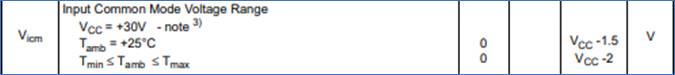
Knowing the
non-inverting input, Vp, is at the same potential as
the inverting input, Vm, (called the common-mode
voltage, VCM) what are the maximum and minimum allowable common-mode voltages?
The maximum common-mode voltage is VCC-1.5V which is 3.5V and the
minimum is 0V
Support your
answer with an entry from the electrical characteristics table in the
datasheet.
As shown here on the data sheet for 5V VCC+ and 0V VCC- the
maximum Vcm would be Vcc -
1.5V = 3.5V. The minimum Vcm would be 0V. But this
OP-AMP can have a VCC+ up to 30V. The max Vcm at VCC+
30V is 30 - 1.5V = 28.5V at (25![]() C)
C)
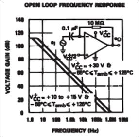
What is a good
estimate for the op-amp's open-loop gain?
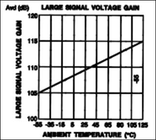
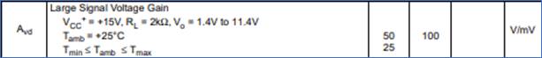
According to the plot below (Open Loop Frequency Response) at 10Hz
frequency we have a gain of about 100dB = 20log(x) which is equal to 100k. This
is supported characteristic table which states that the gain is about 100V/mV
which is 100k at (25![]() C). We can see in the plot
below (Large Signal Voltage Gain) that the Gain does not change to much in
reasonable temperatures.
C). We can see in the plot
below (Large Signal Voltage Gain) that the Gain does not change to much in
reasonable temperatures.
Support your
answer with a plot from the datasheet and an entry from the electrical
characteristics table.
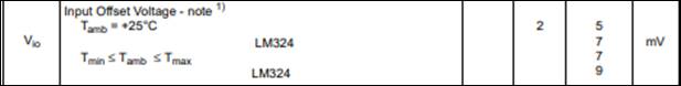
What
is a good estimate for the offset voltage?
For
worst case design what value would you use?
According to the Electrical Characteristics table a good estimate
for the offset voltage would be 2mV. The worst-case design would be 9mV. These
values are based on a VCC+ = 5V and at 25![]() C.
C.
Experiment
1: Building OP-AMP Circuit 1
Build, and test, the following
circuit. Note that a precise value for the 5k resistors isn't important. You
can use 4.7k or a 5.1k resistors.
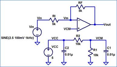
What is the
common-mode voltage, VCM? Does VCM change? Why or why not?
The common-mode voltage is defined as the average of the two
inputs of the op-amp in this case it would be 2.5V this value is calculated
with a voltage divider; which has an input voltage of 5V and two 10k resistors.
The capacitors are open in DC operations.
Vcm = Vcc * (10k/20k) = 2.5V
What is the
ideal closed-loop gain?
The ideal closed-loop gain for an inverted op-amp would be
–(RF/RI) which in this case would be equal to -1. The output waveform would
just be Vin but out of phase by 180![]()
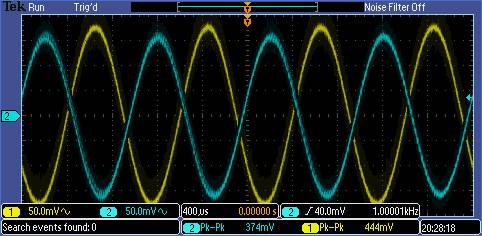
Oscilloscope
measurement with -1 gain
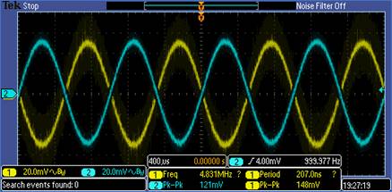
What is the
output swing and what is it centered around?
The output swing is 100mV in the picture above we can see that it
is about 121mV.
What
happens if the input isn't centered around around
VCM, that is, 2.5 V?
Provide
a detailed discussion illustrating that you understand what is going on.
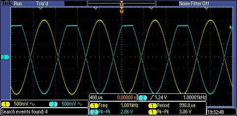
If not centered around 2.5V (VCM) either below or above the
waveform might clip because it could run into +Vcc or
-Vcc sooner than expected which would cause the
waveform to clip. We can see in the picture below that the waveform clips
because input is more than 2.5V. Since the waveform is centered at 2.5V and the
amplitude is more than 2.5V it clips at 5V since that is the maximum allowable
range of voltage. This happens because VCC+ is equal to 5V.
Oscilloscope
waveform clipped
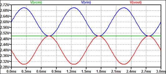
Ltspice simulation
not centered at 2.5V
What is the
maximum allowable input signal amplitude? Why?
The maximum allowable input signal amplitude is 2.5V. The waveform
has an amplitude of 2.5V and it is centered around 2.5V if the input exceeds
this value it will surpass the VCC which is 5V.
What is the
maximum allowable input signal if the magnitude of the gain is increased to 10?
Why?
The maximum allowable input signal if the gain is increased to 10
is 250mV. If the gain is increased to 10, (Vout/Vin)
= 10 so the new allowable input value would have to be 0.1 * 2.5 =250mV. This
would take care of the increase in gain.
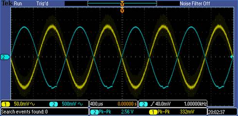
Example
of how clipping occurs at 250mV with a gain of 10
What is the
point of the 0.01 uF capacitors from VCC and VCM to
ground? Are these values critical or could 0.1 uF,
1,000 pF, 1 uF, etc. capacitors be used?
These capacitors are known as decoupling capacitors. They help with
the amount of noise that is seen in the waveform. They do not affect the
voltage divider because they act as an open in DC. The values that are used are
not important 0.1uF, 1000pF, 1uF these can all be used.
The data sheet shows that this op-amp has an input bias current that flows out of the op-amp's inputs of typically 20 nA. This current flows out of both the non-inverting and inverting inputs through the resistors connected to these inputs. Show how the operation of the circuit can be affected if, for example, R1 and R2, are much larger. Explain what is going on. What is the input offset current? What does this term describe?
Our Vcm
would change depending on the size of the resistors. Even if the current is
very small the resistors could be large which would cause a notable voltage drop. This voltage will add to Vcm
and could clip the output since the allowable max input is 2.5V

The input offset current is the current offset of the two input
terminals. Here are both the offset current (below) and the input bias current
(above) the max values are shown in the column before the nA.
Average value is shown before that. Values are all with VCC+ = 5V, VCC- = 0,
and at room temperature.

30MEG
resistors showing voltage drop
The
amplitude of the waveform gets smaller because the little bit of input bias
current causes a notable voltage drop with the big
30MEG resistors.
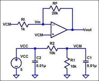
Experiment 2: Building
Circuit 2 with 4 Different OP-AMPS

Explain how the following circuit can be used to measure
the op-amp's offset voltage.
In
an ideal op-amp the two input terminals would be equal so VM would equal VCM so
there would be no current flowing through the R1 resistor. The closed loop gain
for an inverting op-amp is –(Rf/RI) which is -20. The offset could then be:
![]()
To
measure small offset voltages increase the gain by
increasing RF to 100k or larger. Explain what is going on. Measure the offset
voltage of 4 different op-amps and compare them.
For
this experiment we used 4 different op-amps to see the difference in offset. We
used the same LM324 chip but 4 different chips and we
still got a different offset for each of the different measurements. Here we
can see as mentioned in class that even if we are using the same LM324 chips we
can still have different offsets.
Here
we wanted to measure small offset voltages so we increased the gain by increasing RF to
100k. The four different OP-AMPS are shown below.
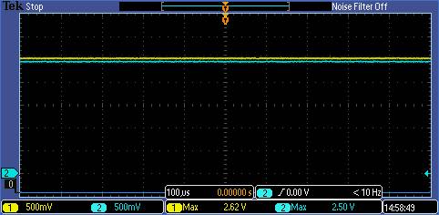
Offset of 1mV Offset of 2mV

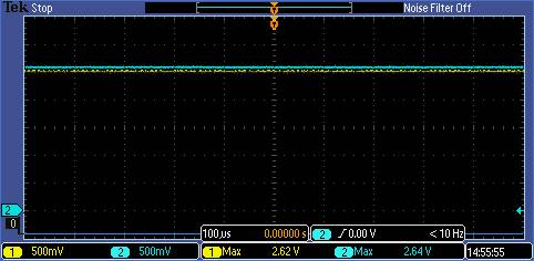
Offset of 1.2mV
Offset of 1.6mV

Here we can see that even though we are using
the same LM324 chip but 4 different chips we still get a variation in the
offset. Like we learned in class the only way we could get away with having the
same offset would be to use chips that were manufactured the same by the same
people maybe even the same date.
Conclusion:
This lab was very helpful for my understanding about OP-AMPS it helped reaffirm
the information that I learned in Circuits 1. As well as taught me new
information like voltage offset and how it can affect the circuit. We also
learned how useful a data sheet can be to find a lot of different information
that we can use to better understand the chips being used. I relearned the
closed loop gain and how to derive it. As well as how the open loop gain
affects the output with the two input node voltages.