Lab
X - ECE 421L
Authored
by Clayton Frister,
FristerC@unlv.nevada.edu
February 14, 2017
- Knowing
the non-inverting input, Vp, is at the same potential as the inverting
input, Vm, (called the common-mode voltage, VCM) what are the maximum
and minimum allowable common-mode voltages?
- Support your answer with an entry from the electrical characteristics table in the datasheet.
According
to the data sheet the minimum lower
end is 0V and the upper end of the VCM is VCC-1.5, but as said in the
footnote included, the input common mode voltage of either input should
not be allowed to go negative by more than 0.3v.


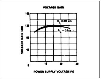
- What is a good estimate for the op-amp's open-loop gain?
- Support your answer with a plot from the datasheet and an entry from the electrical characteristics table.
From the data sheet we see that the large voltage gain is 100V/mV.

The plot below is a plot of the voltage gain.
- What is a good estimate for the offset voltage?
- For worst case design what value would you use?
To
start with, I would look at the data sheet and see the section called
Vio, which is the input offset, and go with the listed 2 mV. But
keeping in mind its max input offest is 9mV. 
Build,
and test, the following circuit. Note that a precise value for the 5k
resistors isn't important. You can use 4.7k or a 5.1k resistors.

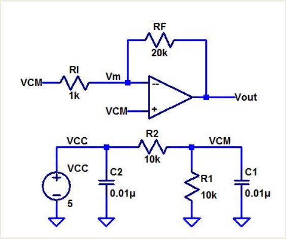
- What is the common-mode voltage, VCM? Does VCM change? Why or why not?
The
common-mode voltage in the circuit above is a voltage offset that is
"common" to both the inverting and noninverting inputs of the op-amp.
VCM in this circuit is set up as a voltage divider to keep the positive
and negative terminals of the op-amp at the same potential and sets the
offset voltage output swing so it does not change.
What is the ideal closed-loop gain?
1.
Ideal closed- loop gain -RF/Rin = -5k/5k = -1.
You can see the output (ch 2) is the same amplitude but 180 degrees phase
difference.

What is the output swing and what is it centered around? What happens if
the input isn't centered around VCM, that is, 2.5 V? Provide a detailed
discussion illustrating that you understand what is going on.
The
output swing of an op-amp is basically a range of voltage that the
output signal will be. Lets analyze our circuit, our input voltage is
1V with a gain of -1. And our rail voltages are 0 and +5. We also have
a 2.5v offset, which means our signal is shifted upward to 2.5v as the
center of our waveform. Also, because the gain is a negative one the
phase is shifted 180 degrees. The amplitude on the output does not
change because of the gain due to the ratio of the input and feedback
resistors. If we didn't have the circuit centered around the 2.5v mark
then the op-amp would be pushing its output close to the rail voltage
which will cause the signal to clip. If we change the offset closer to
the 0 volt, or ground rail, voltage we will see it start to
clip the upper portion of the signal. It clips the upper portion
because it is 180 degrees out of phase. If we change the offset
closer to the 5 volt positive rail voltage we will see it clip the
bottom part of the signal due the the 180 degree phase shift.
(The
first set of pictures below are of my simulations. I did the
simulations to compare my experimental results to because at first I
wasn't sure if what I was doing was correct, but the simulations seem
to have behavior as the experiments done in the lab.)

 2.5v Offset Simulation
0v Offset Simulation
2.5v Offset Simulation
0v Offset Simulation

5v Offset Simulation


Output Swing with 1.3v
Offset
Output
Swing with 4.3v Offset
What is the maximum allowable input signal amplitude? Why?
Since
we are at maximum output swing at 2.5 and the rail voltage is only 5
volts then we are at the maximum allowable voltage. As you can see from
the previous pictures that as soon as we start adjusting the input
voltage either up or down we start clipping our output signal.
What is
the maximum allowable input signal if the magnitude of the gain is increased to
10? Why?
Since
we've seen that the signal gets clipped the closer it comes to the rail
voltage, if we were to increase the gain by 10 then we would for sure
clip the signal since we are at maximum output swing. Therefore in
order to be able to increase the gain by 10 we would have to reduce the
input voltage by a factor of ten (divide the input voltage by 10 and
use that value as our input voltage).
What is
the point of the 0.01 uF capacitors from VCC and VCM to ground? Are these
values critical or could 0.1 uF, 1,000 pF, 1 uF, etc. capacitors be used?
These
capacitors are put in place to get rid of any frequency noise that may
disrupt or "dirty" the signal. These capacitors decouple the DC signal
from the AC so that a more stable signal flows within the circuit.
The only effect the values will have on the circuit is how well
they attenuate, or get rid of, the noise in the circuit.
The data
sheet shows that this op-amp has an input bias current that flows out of the
op-amp's inputs of typically 20 nA. This
current flows out of both the non-inverting and inverting inputs through the
resistors connected to these inputs. Show how the operation of the circuit can
be effected if, for example, R1 and R2, are much larger. Explain what is going
on.
This
circuit is operating with both resistors of the same value, which means
that they are allowing the best possible output swing for this circuit.
If we were to make R1 or R2 much larger then the output of the circuit
would start to see a gain in the output which would cause the
voltage to clip. Below is a simulation of the circuit with
an R2 value of 200k and the ouput clipping.

What is
the input offset current? What does this term describe?
Input
offset current is the difference in input currents between the two
inputs. In the data sheet we can see that the input offset current for
this op-amp is 2nA.
 Explain how the following circuit can be used to measure the op-amp's offset voltage.
- Note that if the output voltage is precisely the same as VCM then the op-amp has no offset voltage (this is very possible).
- To measure small offset voltages increase the gain by increasing RF to 100k or larger. Explain what is going on.
- Measure the offset voltage of 4 different op-amps and compare them.
To
measure the offset voltage of the op-amp we first have to find out what
the gain of the circuit is. In this particular ciruit the gain is
RF/RI, which equals 20. Then we have to measure the VCM and the output
of the circuit and find the difference, and then divide by the gain.
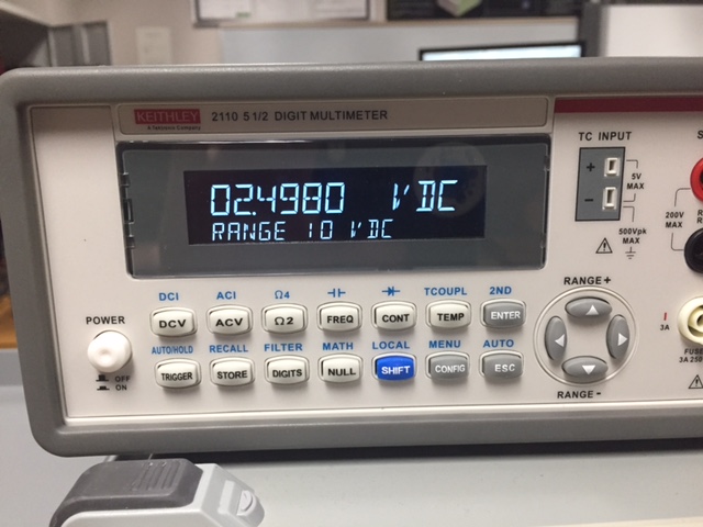
Op-Amp 324


VCM
Output
Offset voltage = (2.4961-2.4940)/20 =0.105mV
Op-Amp 348


VCM
Output
Offset Voltage = (2.5025-2.5267)/20= -1.21mV
Op-Amp 339

VCM
Output
Offset Voltage = (2.4980-2.4928)/20 = 0.26mV
Op-Amp tl081


VCM
Output
Offset Voltage = (2.3859-1.9214)/20 = 23.2mV
Back to Lab 3 Folder
Back to FristerC
Back to Students Folder