Lab 9: Design of a Beta-Multiplier Reference (BMR) using the CD4007 - ECE 420L
Authored By: Joey Yurgelon
Email: yurgelon@unlv.nevada.edu
April 21st, 2015
Pre-lab Work:
- This lab will use the level=1 MOSFET model created in lab 8 and, again, the MOSFETs in the CD4007.pdf CMOS transistor array.
- Design and simulate the operation of a BMR that biases the NMOS devices so that they have a gm of 20 uA/V
- Use a simple (big) resistor to VDD for the start-up circuit (explain how the addition of a resistor ensures start-up).
- When
the BMR is operating the current in the big resistor should be much
smaller than the current flowing in each branch of the BMR
- Write-up,
similar to a homework assignment, your design calculations and
simulation results. (This will count as the pre-lab quiz.)
- Ensure that you show the following in what you turn in:
- Hand calculations
- Operation as VDD is swept from 0 to 10 V
- Vbiasn
should stabilize (be constant) after VDD hits a minimum value (estimate
this value of VDD assuming VGS/VSG is a threshold voltage and
VDS,sat/VSD,sat is zero).
- Vbiasp should follow VDD after VDD hits a minimum value (show this in simulations)
- Unstable operation if too much capacitance is shunting the BMR's resistor (see bottom of page 630)
- Comments comparing the hand calculations with the simulation results
Lab Description:
- Students
will characterize use the techniques described in class to characterize and build a BMR.
Lab Requirements:
In this lab you may need to use two,
or more, CD4007 chips from the same production lot (see date code on
the top of chip) to ensure using a BMR to bias a current mirror is
possible. If the CD4007 chips are not from the same production lot they
will not "match" so current mirrors will not be possible.
- Build your BMR design and characterize it as you did in the pre-lab
- You
expect the BMR to become unstable if there is a large capacitance
across the resistor, such as a scope probe (important), so care must be
exercised
- Use your BMR to bias, and thus create, a:
- NMOS current mirror
- PMOS current mirror
- Measure how the current varies through each current mirror as the voltage across the mirror changes.
- Of
course the current in the NMOS (PMOS) current mirror goes to zero as
the voltage on the drain of the output device moves towards ground (VDD)
- Using these current mirrors drive two gate-drain connected transistors
- For the first experiment use the NMOS current mirror to drive two PMOS gate-drain connected devices.
- Use
the voltages on the gate-drain connection of the two devices to bias a
cascode current mirror (characterize this mirror as before)
- For the second experiment switch, that is, use the PMOS current mirror to drive two NMOS gate-drain connected devices.
- Again, use these two voltages to bias an NMOS cascode current mirror then characterize.
Experimental Results:
Exercise #1: Pre-Lab BMR Design
-
The design just
followed similar suit to the ones put forth in the homework. To develop a K
value, however, we will have to parallel multiple MOSFETs together as we cannot
directly change the W and L of the devices. The W/L used was based on the
values used in Lab 8. The large resistor
works as a start up by leaking a small amount of current into the NMOS gates.
This gives them just enough juice to snap into operation, and out of the dead
state where they are held at ground. My simulation current was less than that of
my hand calculations, but since the simulation uses an already estimated SPICE
model, it would make sense that they would not line up exactly.
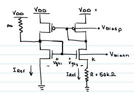
Hand-Drawn BMR Schematic and Calculated Resistor | Theoretical BMR Hand Calculations |
LTSpice Simulated BMR
| LTSpice Simulated VDD Sweep |
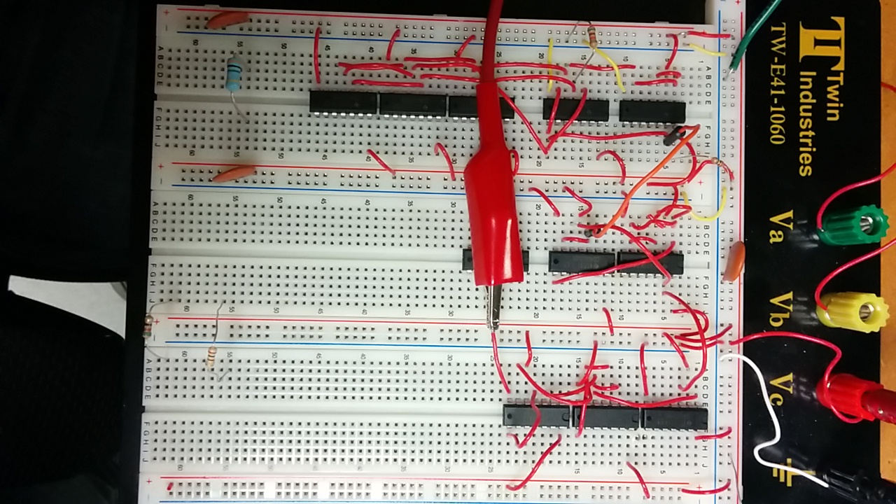
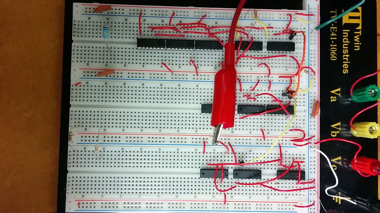
Exercise #2: BMR Builds and VDD Characterizations- These
circuits were quite a headache to build due to the layout of the
CD4007, but luckily we were able to get respectible results on the BMR
as one can see from the VDD sweep characterization below. In order to
get reasonsable results, but we had to use a vast amount of CD4007
chips. As one would expect, with each added chip, we introduce various
error into the system due to various secondary effects which could then
have adverse effects on the caparison between theory and experimental.
We noticed that our curves were not going to be in full agreement with
theory, but after double checking our schematics and builds
various times, these were the results that we obtained.
- For
the BMR, we
took the voltage across the 50k resistor and then divided by the value
to obtain the current flowing in the BMR. This method was changed for
the remaining circuits as we simply added a ammeter in series
with the circuit so that we could find the drain current flowing
through it. The BMRs purpose is to provide a "supply independent"
biasing structure that can then bias various current mirror loads and
so on. As we know from simulations, theory is a far more idealized
situation and is free from the faults of outside influence. These
outside influences played a role in our circuits. With each added
structure to the BMR (current mirror then cascode), we felt that our
VDD sweep curve varied with each added stage, and performance only
decreased.
- The
current mirror was biased from either the gate of the NMOS or PMOS of
the BMR, depending on which type of current mirror is needed, and then
was used to bias up a N/PMOS to sink or supply current to two
gate-drain connected mosfets (opposite of which is being source
MOSFET). The gates of the gate-drain connected devices can then be
connected to another set of the same type of mosfets to construct the
structure noted below in the 'Cascode Builds' below.
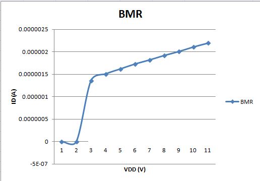
BMR Current Variation with VDD | BMR Breadboard Build |
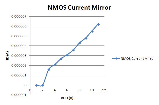
NMOS Current Mirror Driven by BMR | 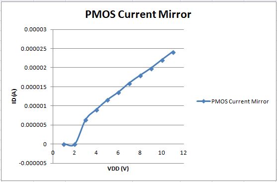
PMOS Current Mirror Driven by BMR |

NMOS Cascode Current Mirror | 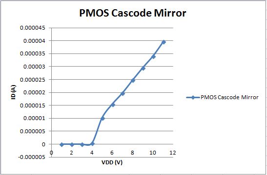
PMOS Cascode Current Mirror |

NMOS Cascode Current Mirror Build | 
PMOS Cascode Current Mirror Build |
Return to EE 420L Labs

