Lab 6: Single-Stage Transistor Amplifiers ECE 420L
Authored By: Joey Yurgelon
Email: yurgelon@unlv.nevada.edu
March 17, 2015
Pre-lab Work:
- This lab will utilize the ZVN3306A and ZVP3306A MOSFETs.
- Review these datasheets and become familiar with these transistors.
- Verify that the simulations seen in lab6_sims.zip reasonably model the behavior of the transistors' ID v. VGS, ID v. VDS, and gm v. VGS curves.
- Finally, watch the video single_stage_amps and review single_stage_amps.pdf
Lab Description:
- Students
will understand how to experimentally calculate the input and output resistances of single-stage transistor amplifiers.
Lab Requirements:
- Below are schematics for NMOS and PMOS source followers amplifiers (also known as common-drain amplifiers).
- In your lab report discuss the operation of these circuits.
- Simulate the operation of these amplifiers.
- Hand
calculate, and then verify your hand calculations with experimentation
and simulations, the gains and the input and output
resistances ensuring that your test signals are at a high enough
frequency that the caps have negligible impedance but not so high that
the gain is dropping off.
- If
you build this circuit using electrolitic capacitors, assuming the
input AC signal swings around ground, put the "+" terminal of the cap
on the gate of the MOSFET. Please indicate, in your lab report, that
you understand why the capacitor is connected this way.
- In your lab report discuss, in your own words, how to measure the input resistance.
- For measuring the input resistance add a resistor equal to the value you calculated between the input voltage source and the amplifier.
- Measure
the peak AC current through this added resistor by taking the
difference in the peak AC voltages across the resistor (on one side is
the input voltage signal and the other side is the connection to the
amplifier's input capacitor) and then dividing by the resistor's value.
- Measure the peak AC voltage on the input of the amplifier (the left side of the capacitor).
- Dividing this peak AC voltage by the peak AC current through the added resistor is the amplifier's input resistance.
- Again, in your lab report discuss how to measure the output resistance.
- For
measuring the output resistance, add a resistor equal to the value you
calculated in series with a big capacitor (to avoid messing up the
biasing) from the amplifiers output to ground.
- Measure the peak AC current through this added resistor.
- Measure
the peak AC voltage (remove the DC component) on the gate of MOSFET and
the peak AC voltage on the source of the MOSFET. The difference in
these two AC voltages is the peak AC gate-source voltage of the MOSFET.
- Dividing
this peak AC gate-source voltage by the peak AC current through the
added resistor is the amplifier's output resistance.
Experimental Results:
- Note:
Due to the nature of the waveforms used to determine input/output
resistance (Output halved due to divider effect), only the output
resistance waveforms were shown. For the first four amplifiers, the
input resistance is theoretically the same between CD and CS.
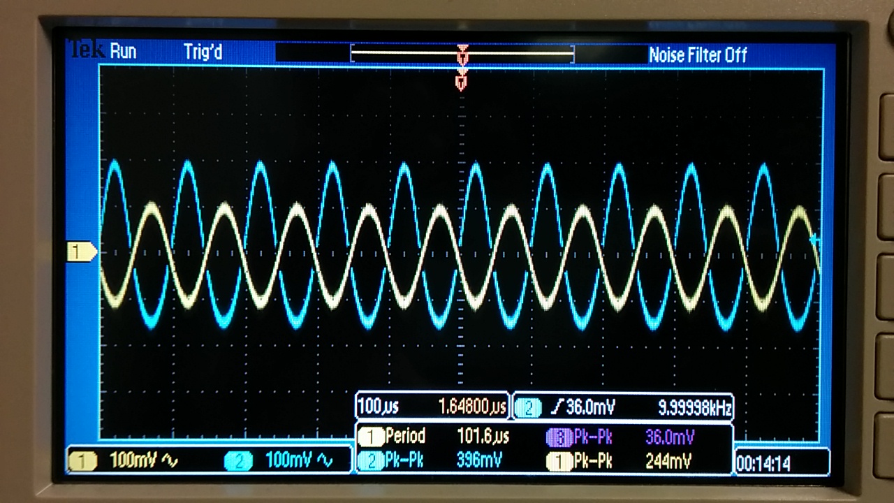
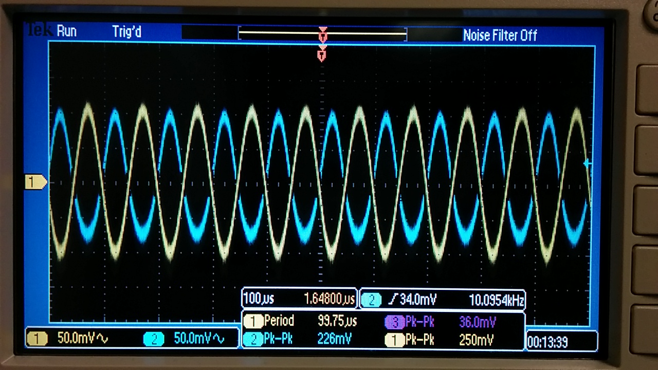
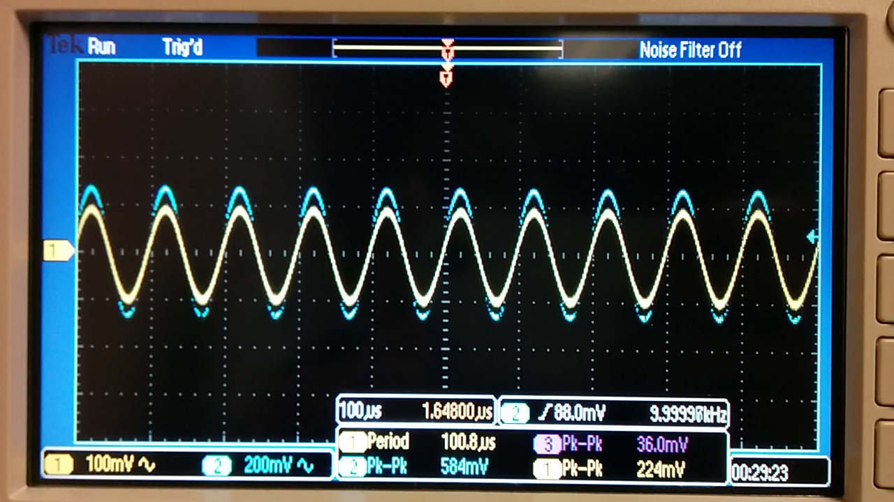
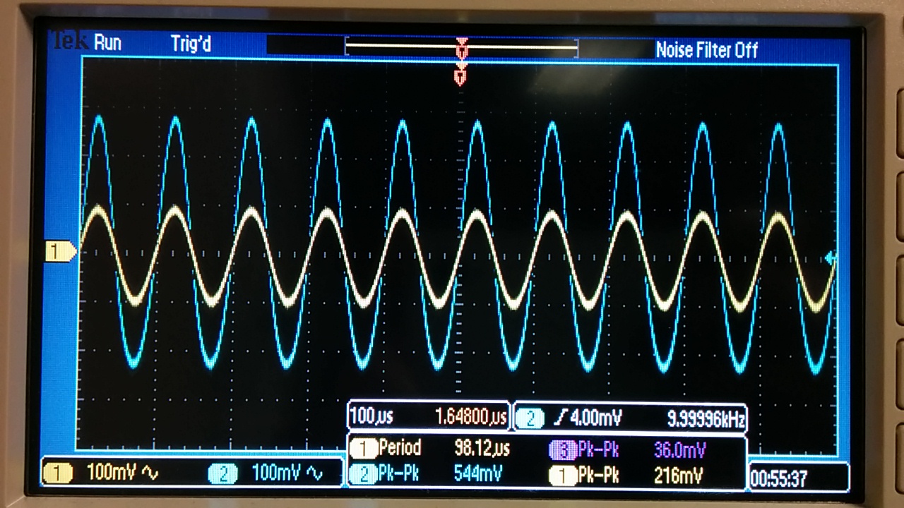
Exercise #1: Experimentally determine the input and output resistances of the common-drain amplifiers. Common Drain (CD).
- The
first set of amplifiers that needed to be built in this lab are known
as Common Drain (CD). They are characterized by a gain of nearly 1x,
low input capacitance, and high input impedance. For these amplifiers,
the mosfets are biased by the voltage dividers infront of the gates
which in combination of the resistor in the source, sets the Gate-Souce
voltage at saturation level. The input is AC coupled so that the input
does not disrupt the DC biasing. The output is taken from the source of
the amplifier. After determining biasing, and the AC current through
the mosfets, the input/output resistances are important parameters to
determine.
- To determine the input resistance,
we need to refer to our hand calculations (seen below), and place the
value determined between the input voltage source and the amplifier.
One would then determine the AC current through this added resistor by
measuring both sides, and dividing by the resistance. From there, one
can simply take the peak input voltage and divide by the AC current
determined. This will result in the experimental input resistance. The
following formula can be determined: Rinput = (Vinp)/(ACI) where Vinp
is the peak input voltage, and ACI = (Vr)/Radded or the voltage drop
accross the added resistor divided by its resistance. To verify the
results, place the experimentally determined input resistance between
the input voltage source and the amplifier, and measure the voltage at
the gate and source. One should see a voltage divider effect, and see
the output halved.
- To determine the output
resistance, we need to once again take the result from our our hand
calculations below, but instead of placing the resistor at the input,
we will place it in series with a big capacitor from the amplifiers
output to ground. We will then measure the AC voltage across the added
resistor, and then divide the by added resistance to determine the peak
AC current through the resistor. One will then need to determine the
peak AC voltage which is determined by measuring the voltage at the
gate of the mosfet as well as at the source, and then subtracting them.
From here, one will simply need to divide by the peak AC voltage by the
peak AC current to determine the experimental output resistance. The
following formula help illustrate the point: Iacp = (Vr)/Radded, Vp =
Vg - Vs, Rout = Vp/(Iacp) where Iacp is the peak AC current, Vr is the
voltage across the added resistor, and Vp is the peak AC voltage.
Similarly to the input resistance, one should be able to see a voltage
divider effect in which the output is divided in half.
| Experimental Input Resist CD | Experimental Output R |
| NMOS | 75.25kOhm | 52.46 Ohm |
| PMOS | 80kOhm | 493.4 Ohm |

Common Drain Hand Calculations |
NMOS/PMOS Common Drain Gains | Common Drain Output Resistance |

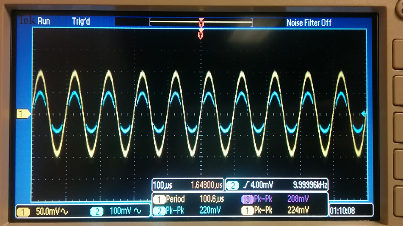
NMOS Common Drain Experimental Gain < 1x | 
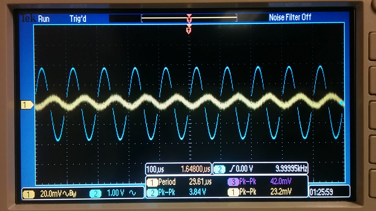
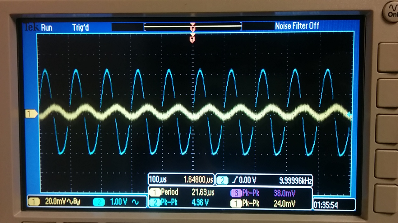
NMOS CD Experimental Output Resistance |

PMOS Common Drain Experimental Gain < 1x | 
PMOS CD Experimental Output Resistance |
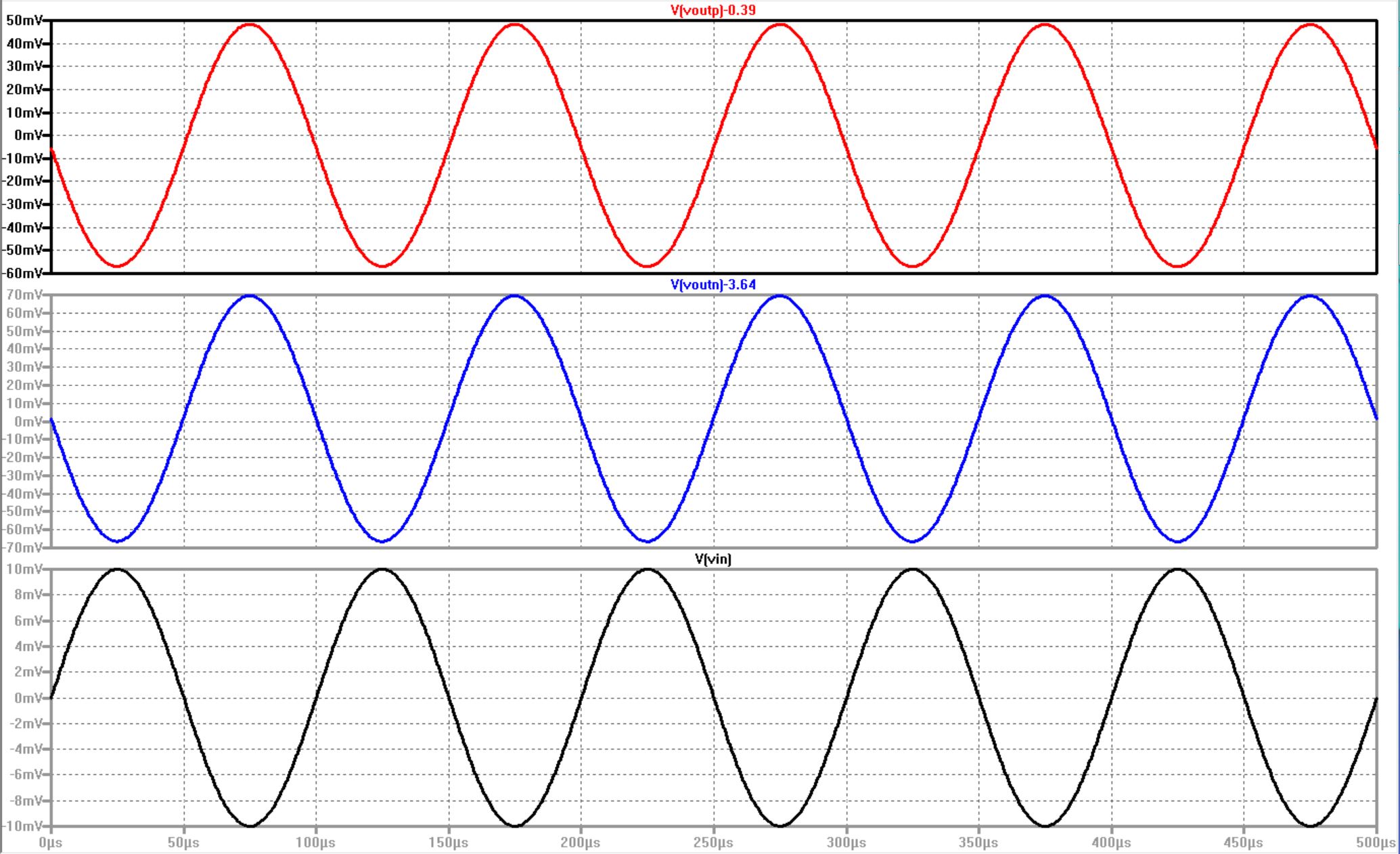
Exercise #2: Experimentally determine the input and output resistances of the common-source amplifiers. Common Source (CS).- Below
are two common source amplifiers. Both are are biased by the voltage
divider located at the gate as well as the resistors in the drain and
the source. This will set our bias, and will be able to hold the mosfet
in the saturation region. The added capacitors only come into play when
looking at the AC operation of the circuit. They should be large enough
to appear as shorts, and prevent any issues in the biasing when
applying an AC input voltage. The common source, unlike the common
drain, is characterized by the gain of the amplifier. It is typically
much large than 1x. In this case, Rsn or Rsp can be changed to either
increase or decrease the gain. By increasing Rsn or Rsp, we are
effectively decreasing the gain in the common source amplifier. This is
due to the fact that the gain, which can be seen below, contains an
Rsn/Rsp term in the denominator, and thus by increasing the value in
the denominator, we decrease the gain. The converse is also true.
| Experiment Input Resistance | Experimental Output Resistance |
| NMOS | 69.8kOhm | 167.7 Ohm |
| PMOS | 89.2kOhm | 758 Ohm |

Common Drain Hand Calculations |
NMOS/PMOS Common Source Gains | Common Source Output Resistance |

NMOS Common Source Experimental Gain | 
NMOS CS Experimental Output Resistance |

PMOS Common Source Experimental Gain | 
PMOS CS Experimental Output Resistance |
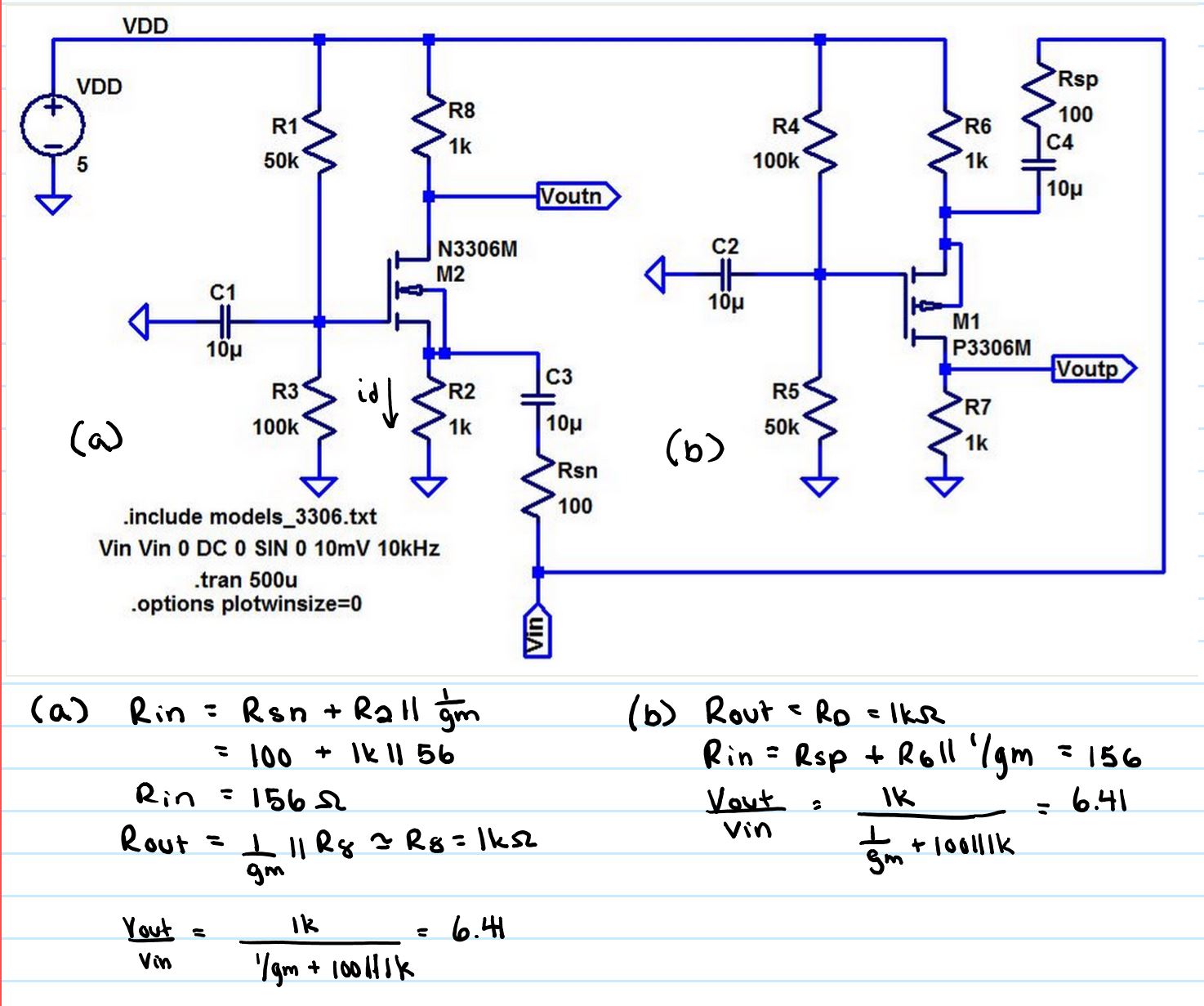
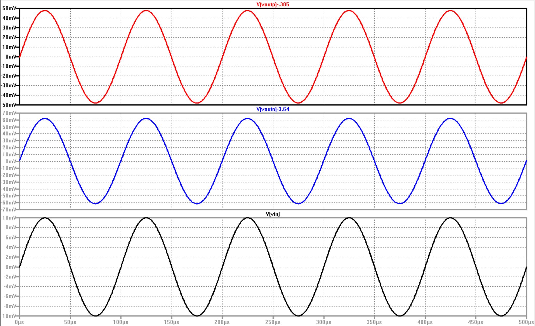
Exercise #3: Experimentally determine the input and output resistances of the common-gate amplifiers. Common Gate (CG).- The
common gate amplifer follows similar suit as the common source. The
difference, however, comes into play with the amplifiers gain which is
no exhibits an 180 degree phase shift, and the input resistance is much
smaller. In the common source and the common drain above, the input
resistance was determined to be 33.3kOhm, but for the common gate, it
is determined to be approximately 156 Ohms. As far as biasing is
concerned, the common gain is DC biased the same as the previous
amplifiers, and coupled with capacitors so that any AC input would not
affect the biasing.
| Experimental Input Resistance | Experimental Output Resistance |
| NMOS | 354 Ohm | 267.18 Ohm |
| PMOS | 557.1 Ohm | 602 Ohm |
Common Gate Hand Calculations |
NMOS/PMOS Common Gate Gains | Common Gate Output Resistance |

NMOS Common Gate Experimental Gain | 
NMOS CG Experimental Output Resistance |

PMOS Common Gate Experimental Gain | 
PMOS CG Experimental Output Resistance |
Exercise #4: Build and analyze the push-pull amplifier- The
push-pull amplifier is biased by the 5 V source voltage. There is no
current through the 100kOhm resistor to the gates which sets the gate
at a voltage to keep both of the mosfets in saturation. The AC voltage
input is coupled by a capacitor to prevent any messing up of the bias.
From the hand calculations below, we can see that we are able to look
at the output resistance of each mosfet, and add them together to
characterize the input/output relationship of the amplifier where the
resistor acts as a gain multiplier. By this result we can determine
that if we were to change this resistor to a much higher value, such as
510kOhm, out gain would increase. This amplifer is good at both
sourcing/sinking current due to the topology at the output. The PMOS
has the ability to source current when on, and the NMOS can sink
current when the on.

Push-Pull Hand Calculations |

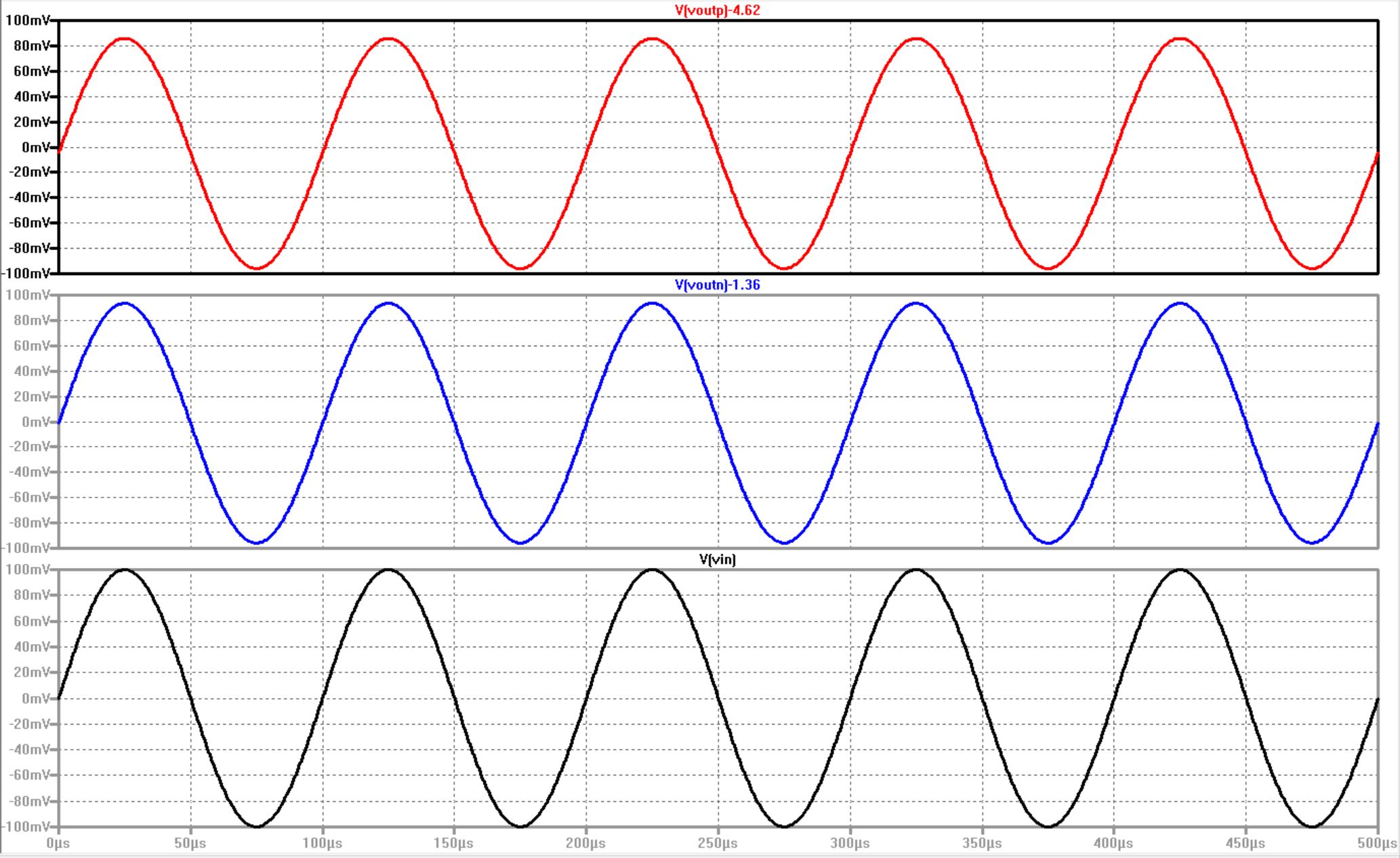
Push-Pull Spice Schematic | Push-Pull Output Resistance |
Push-Pull with 100kOhm | Push-Pull with 510kOhm |
Return to EE 420L Labs


