Lab 5: Op-Amps III, The Op-Amp Integrator ECE 420L
Authored By: Joey Yurgelon
Email: yurgelon@unlv.nevada.edu
February 27, 2015
Pre-lab Work:
Lab Description:
- Students
will understand how the op-amp integrator functions, and will know how to design one for practical purposes.
Lab Requirements:
For the following questions and experiments assume VCC+ = +5V and VCC- = 0V.
- Calculate the frequency response of the following circuit. Ensure you show your clear hand calculations.
- What can you neglect to simplify the calculation?
- Does the circuit work if you remove the 100k? Why or why not?
- Does the 100k have much of an effect on the frequency response?
- Verify your calculations with experimental results.
- Show, at the unity-gain frequency of the integrator, that the input and the output have the same peak values.
- Is the phase shift between the input and the output what you expect? Why or why not?
- Next, design, simulate, and build a square-wave to triangle wave generation circuit.
- Assume the input/output frequency is 10 kHz and the output ramp must swing from 1 to 4 V centered around 2.5 V.
- Show all calculations and discuss the trade-offs (capacitor and resistor values, input peak, min, and average, etc.)
Experimental Results:
Exercise #1: Calculate the frequency response of the following circuit. Ensure you show your clear hand calculations.
- By
plugging in values of the design, one can see that the unity gain
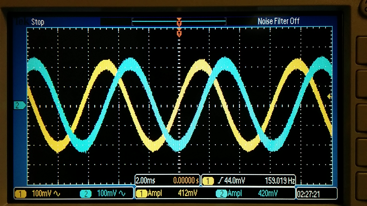
frequency of the op-amp integrator occurs at approximately 159 Hz. This
result is confirmed in our measurments. The phase shift between the
input and the output should be 90 degrees through out. This result can
be clearly seen in our sine output wave below. With a time delay of
approximately 1.8 ms the phase shift can be calculated with the
following formula: Phase = td*f*360. In our case, the phase shift is
calculated to be 103 degrees.
- What can you neglect to simplify the calculations?
- R2 can be neglected in the
circuit. Since R2 is usually a very large value, its only purpose is to
discharge the capacitor and account for any non-ideal DC offset at the
inputs. If we are dealing with a non-ideal op-amp, and there was no R2
introduced in the circuit, the output would saturate at the rails or go
directly to zero depending on whether the offset is positive or negative.
For an ideal case, it is not necessary.
- Does the circuit work if you remove the 100k? Why or why not?
- In the ideal case, we are
assuming that there is not offset voltage, and the output is only based on
the input voltage. Non-ideally, this is not the case. Most op-amps will
have a DC offset which would cause the output to either saturate or drop
directly to ground.
- Does the 100k have much of an effect on the frequency response?
- The R2 does not have a huge
effect on the frequency response. It will serve to shift magnitude
slightly, but one can easily get an idea of the frequency response without
including it.
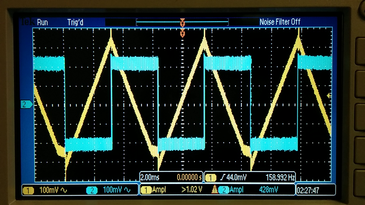
Exercise #2: Next,
design, simulate, and build a square-wave to triangle wave generation
circuit. Assume the input/output frequency is 10 kHz and the
output ramp must swing from 1 to
4 V centered around 2.5 V.- To
start, we took the base circuit made in the first experiment, and
molded it for out application. Since the output is determined as the
following: Vout = -Vin/(sRC) where 1/s represents integration over
time. From this base model of the circuit, we can go ahead and derive
the governing equation in our design, R = ((Vin-Vcm)(T/2))/(del(Y)C).
We chose the capacitor to be 10nF and from the design constrains:
del(Y) = 4-1 = 3, T = 1/10k = 100 uS, Vcm = 2.5V. From this we were
able to calculate R as 333 Ohms. There are quite a bit of trade offs.
For starters, a smaller capacitor results in a larger input resistor
which reduces in DC gain of the circuit, and vice versa. A larger DC
gain causes the input peak to decrease due to saturation at the op-amp,
and lastly the RC time constant of the feedback capacitor/resistor
needs to be considered so that there is constant triangle function. We
had quite a bit of issues matching the voltages at the input terminals
of the op-amp, but once we did, we were able to see more so than not,
expected results.
Return to EE 420L Labs


