Lab 3: Op-Amps I, Basic Topologies, Finite Gain, and Offset - ECE 420L
Authored By: Joey Yurgelon
Email: yurgelon@unlv.nevada.edu
February 5, 2015
Pre-lab Work:
Lab Description:
- Students
will learn the imperfections associated with op-amps as well as the most common topologies.
Lab Requirements:
- Questions for lab can be seen below.
Experimental Results:
Exercise #1: Use the LM324 Datasheet for the following questions.
- Knowing
the non-inverting input, Vp, is at the same potential as the inverting
input, Vm, (called the common-mode voltage, VCM) what are the maximum
and minimum allowable common-mode voltages?
- Support your answer with an entry from the electrical characteristics table in the datasheet.
- The
maximum common mode voltage is VCC - 2. For example, if VCC was set at
5 V, then the maximum common mode votlage would be 3V. The same would
go for the minimum common mode voltage except it would follow VCC - 1.5.
- What is a good estimate for the op-amp's open-loop gain?
- Support your answer with a plot from the datasheet and an entry from the electrical characteristics table.
- A
good estimation of the open-loop gain would be right around 100 dB.
According to the frequency response, the gain (dB) rolls roughly at 20
dB/decade, but at DC values sits at right around 110 dB.
- What is a good estimate for the offset voltage?
- For worst case design what value would you use?
- A
good estimate of the offset voltage is at 7 mV as it lies between the
min and max offset voltages. For worst case design, one would pick the
highest offset voltage which would be at 9mV.
Exercise #2: Build and test, the following circuit. Precise valued resistors are not needed. - What is the common-mode voltage, VCM? Does VCM change? Why or why not?
- The
common mode voltage is 2.5Vdc. No, the VCM does not change because it
is used as a reference for the AC input signal to swing around. It is
created by the 10k voltage divider at the positive input.
- What is the ideal closed-loop gain?
- The ideal closed-loop gain is -Rf/Rin which is equal to 5k/5k = 1 or 0dB.
- What is the output swing and what is it centered around?
- The output is centered around VCM which is set at 2.5V.
- What happens if the input isn't centered around around VCM, that is, 2.5 V?
- If
the input is not centered around 2.5V, then the op-amp's open-loop gain
is not sufficient to pull Vm up to Vp. If the input voltage at the Vp
terminal increases, the output voltages will decrease, and vice versa.
Vp must be appropriately within bound of the positive supply rail.
- Provide a detailed discussion illustrating that you understand what is going on.
- We
have a 5V input at VCC which is voltage divided to 2.5V at the positive
input terminal, Vp. This voltage, then appears at Vm, due to the
infinite open-loop gain of the nearly ideal op-amp. This voltage is
then multiplied by the closed-loop gain of the topology which is
designated -Rf/Ri. In our case, this would be 1x. For AC, Vp is at AC
ground. Consequently, Vm is then at AC ground while the input AC
voltage is multiplied by the same closed-loop gain. In conclusion, the
output is centered around 2.5V with an AC swing of +/- 100mV.
- What is the maximum allowable input signal amplitude? Why?
- Since
our rails are set at 5V, and 0V. We could then swing +/- 2.5V. Anything
larger, will result in clipping of the signal. The maximum allowable
input signal would then be 2.5V
- What is the maximum allowable input signal if the magnitude of the gain is increased to 10? Why?
- By increasing the magnitude of the gain by 10, the largest input signal would be 250mV theoretically.
- What is the point of the 0.01 uF capacitors from VCC and VCM to ground?
- These capacitors are just to decouple the voltages, and detract noise from the power supply.
- Are these values critical or could 0.1 uF, 1,000 pF, 1 uF, etc. capacitors be used?
- These
values could be anything. They are used to hold the voltage at a node
to a specific value to detract from sudden swings. They are just charge
buckets.
- The data sheet shows that this op-amp has an input bias current that flows out of the op-amp's inputs of typically 20 nA.
- This current flows out of both the non-inverting and inverting inputs through the resistors connected to these inputs.
- Show how the operation of the circuit can be effected if, for example, R1 and R2, are much larger. Explain what is going on.
- If
we had a 20nA input bias current on each of the op-amp terminals, using
a large resistor will produce a larger voltage at Vm, and consequently,
Vp. This mismatch of voltages would then change the ouput voltage of
our op-amp.
- What is the input offset current? What does this term describe?
- The
input offset current is the difference between the input bias currents
at Vp and Vm. It describes the mismatch between the two input currents
of the op-amp.

Hand Calculations |
 LTspice Simulated Circuit Exp #1 LTspice Simulated Circuit Exp #1 | 
Simulated Output Waveform
|

DC Offset Voltage of Input/Output - VCM
| 
Input/Output Voltages, Output has 180 phase shift
|

Op-Amp Clipping When DC Sweeps Too High |
Exercise #3: Explain how the following circuit can be used to measure the op-amp's offset voltage.
- The
circuit is just a simple voltage follower with a common mode input. Any
deviation at the output can then be assumed to be an offset located
within the op-amp. Since the voltage is 2.5V, we would idealy see an
output of 2.5V if there was no offset associated with the op-amp.
- Note that if the output voltage is precisely the same as VCM then the op-amp has no offset voltage (this is very possible).
- To measure small offset voltages increase the gain by increasing RF to 100k or larger. Explain what is going on.
- Measure the offset voltage of 4 different op-amps and compare them.

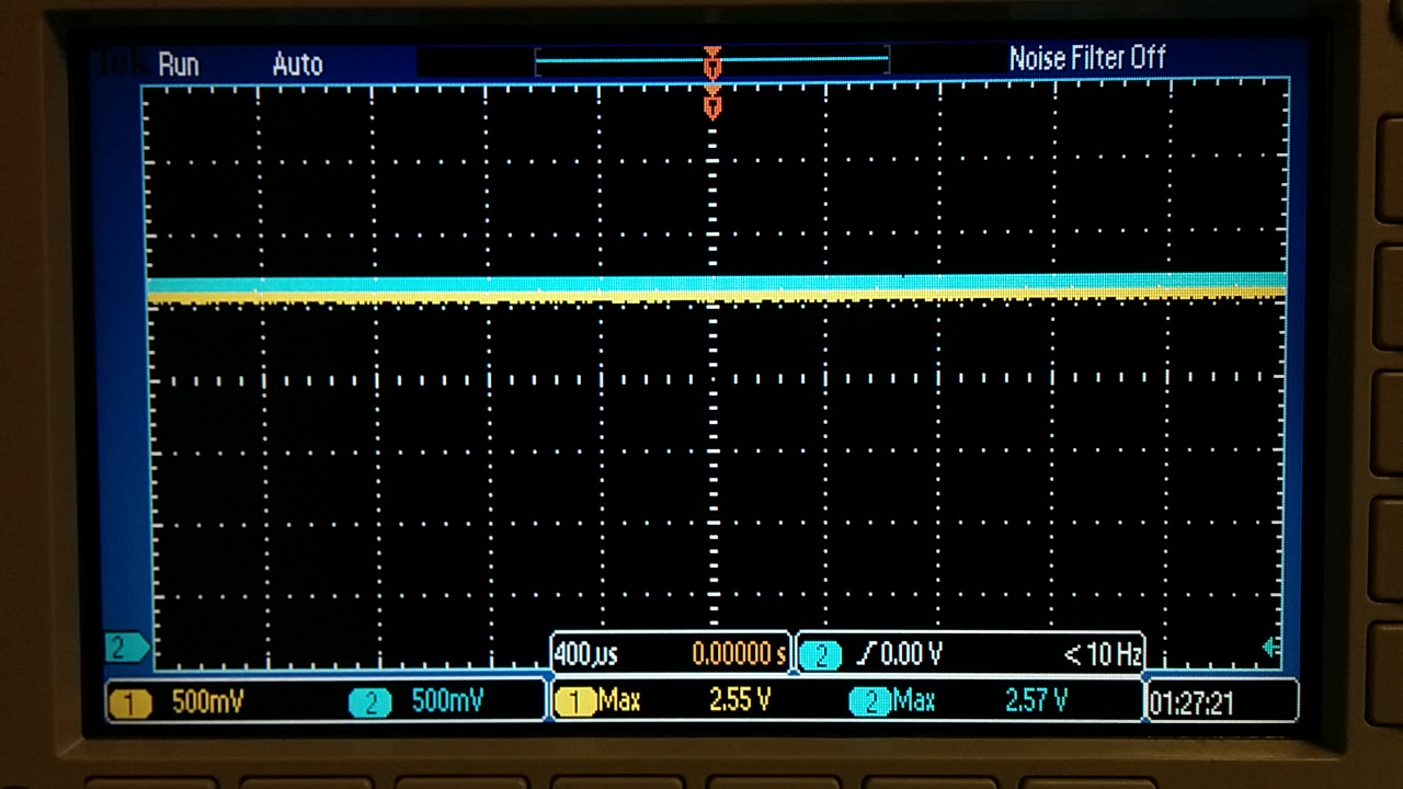
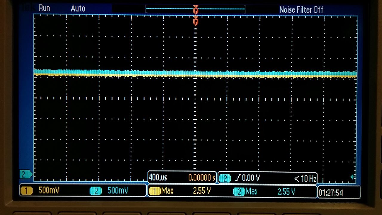
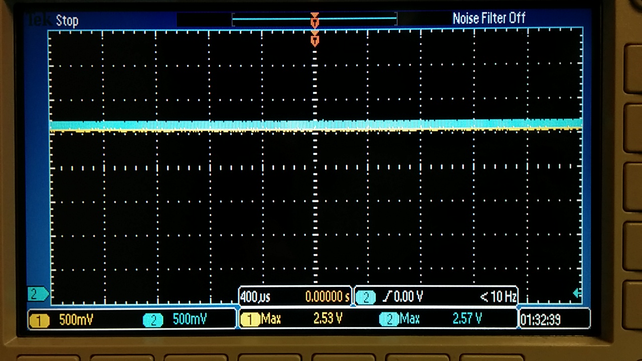
Op-Amp #1: Offset voltage of 20mV | 
Op-Amp #2: Offset voltage of 0mV |

Op-Amp #3: Offset voltage of 20mV | 
Op-Amp #4: Offset voltage of 40mV |

Ideal Amplifier With No Offset - Output = VCM |

LTSpice Circuits of Various Op-Amp Offsets | 
LTSpice Sims of Various Op-Amp Offsets |
Return to EE 420L Labs
