Final Project - ECE 420L
Authored
by Steven Leung
5/5/15
leungs@unlv.nevada.edu
Lab
description
Project - using
as many diodes, resistors, and capacitors as needed, along with two
CD4007 chips from the same production lot (see date code on the top of
chip) to ensure current mirrors are possible, design and build a
bandgap voltage reference (BGR). Your report, in html, should detail
your design considerations, simulation results (using the models you
generated in lab 8), and measured results showing the BGR's performance (how the reference voltage changes with VDD). It would be good, but it's not required, if you could also characterize the BGR performance with temperature.
Design Considerations
The
most important concept to design a band gap reference is the fact that
when a constant current is fed thought the resistor, the voltage drop
across it is constant. Therefore, if we can generate a constant current
through a resister for any given input voltage (VDD), we can use
the voltage across that resistor and use it as a constant voltage
source.
To
generate a constant current is one of the first circuits we looked at
in an analog electronics class, beta multiplier. A beta multiplier
(BMR) will generate a decently straight current (to get a flatter
current we will need more transistors than are on 2 CD4007
chips), therefore, the voltage across the capacitor will still vary
with changing VDD but not as much to connecting VDD to resistors
directly.
The
next idea to consider is that the voltage across a resistor will
increase with temperature. Therefore, to design a BGR that is
independent of supply voltage and temperature, we will use the idea
that the voltage across a diode decreases with temperature. By combing
resistors and diodes in series, we are able to get a voltage that is
almost independent of supply voltage and temperature.
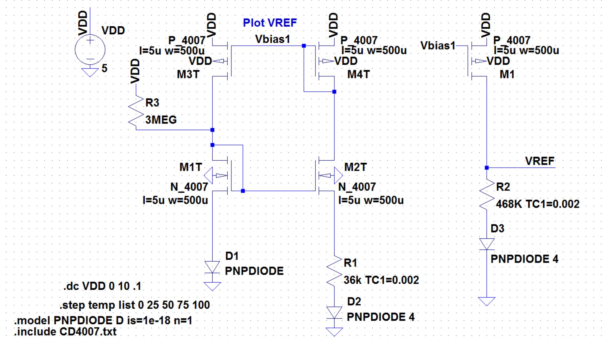
Figure 1 shows the schematic used for this design.

Figure 1 Schematic for BGR |
The
left 2 branches on the schematic in figure 1 are very similar to a BMR
but with diodes connected to the tails since we can only use 2
chips and cannot add k multiples to M2T. Writing a KVL around the tails
and M1T and M2T, we can generate an equation just like we did for the
BMR to pick a k (multiple value) for D2 and current to yield the
value of the resistor needed. (See hand calculations). We picked a k
value of 4 and a current of 1uA. This yielded a resistor value of around
36k. The branch on the right is to take the biasing off the BMR and
adjust the number of resistors in series (increasing the value of the
resistance of R2) such that the voltage drop across the resistor
in series with the K diodes is independent to temperature. This is
done by finding an equation for Vref , taking its derivative with
respect to temperature and setting it equal to 0. This will yield an
equation with one unknown L(number of resistors in parallel). L was
found to be 13.37. Multiplying this to 36k yielded a resistance value
for R2 of about 468K. The purpose of R3 is to ensure that the circuit
will start up correctly.

Figure 2 Hand calculations |
The
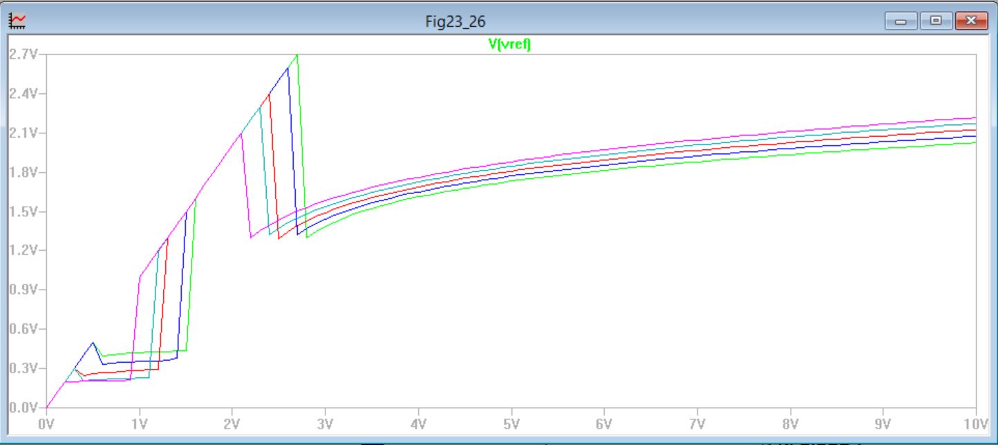
simulations from LTspice are shown in figure 3. Instead of using the
models generated from the previous lab, we found a more complete level
spice model for the CD4007 transistor array online and used that. The model is found here The
first thing to
notice is the voltage is not flat from 0 volts to 10 volts, this is
because there is a minimum voltage needed to put all the transistors
into saturation. The next thing to notice that that voltage reference
point varies a small amount with increasing temperature.

Figure 3 Circuit Simulation |
Below are the experimental results
As
seen from the experimental results, it is close to the simulation in lt
spice. Again, the reason why they curve is not flat is because of
finite output resistance in the BMR. We were not able to test
temperature variation of the circuit since it was hard to get a control
of temperature in the lab.
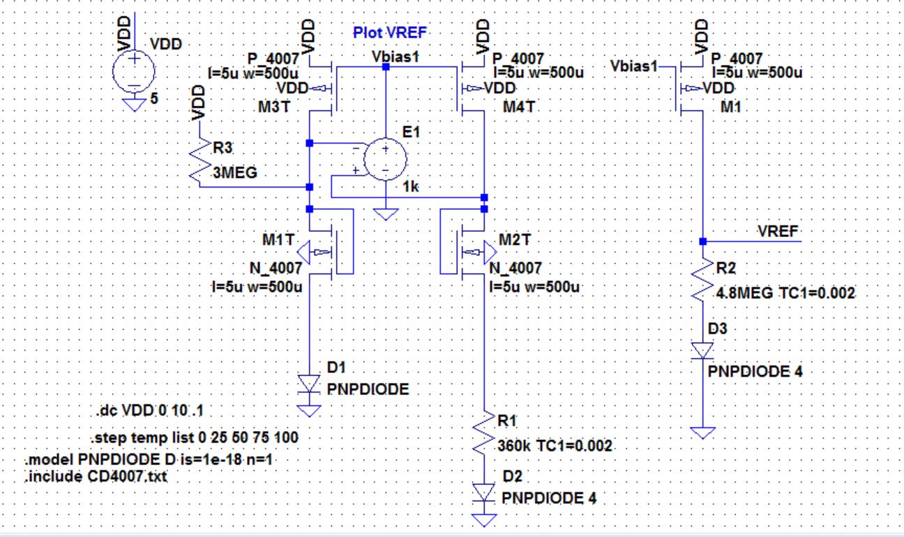
How to improve the design
To improve the design, we can add an amplifier with its inputs
connected to the drains of the NMOS. This will hold those two drains at
the same voltage and therefore increase the output resistance of the
NMOS. A larger output resistance means a flatter current curve and
therefore a flatter voltage curve.
Below is the simulation from adding an voltage controlled voltage source to model an op-amp.
 |  |
| BMR with amplifier schematic | Simulation waveforms |
From
the simulation results, it can be seen that the change in Vref with
respect to VDD is significantly reduced compared to just using a BMR.
We can expect the temperature change to be the same because we have not
changed the values of any resistors or changed the amount of diodes
used. This design can be made even better by using a cascode structure
in the BMR to increase the output resistance even more but this would
require more than 2 chips. We tried using an op-amp to replicate teh
voltage controlled voltage source but were unsuccesful in getting
it to work.
Conclusion
In
conclusion, our design includes a BGR in which it's voltage with
respect to a chaning supply voltage is decreased. With using just to
chips, They're are not many improvements that can be made to make the
curve flatter but at the cost of using more chips, we can increase the
output resistance and therfore have minimal variations in output
voltage with respect to supply voltage.
Add
a return to the listing of your labs