Lab 8:
Chip 7 Project -
ECE 421L
Tyler
Ferreira, ferret1@unlv.nevada.edu
Tyler
Huddleston, huddle10@unlv.nevada.edu
Sharyn
Miyaji, miyajis@unlv.nevada.edu
Raheel
Sadiq, sadiqr@unlv.nevada.edu
The
design directory can be found here: Chip7_f16.zip
This
chip contains:
-
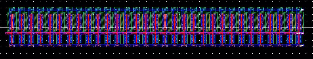
1 31-stage ring oscillator with a buffer capable of driving an off chip
20pF load
-
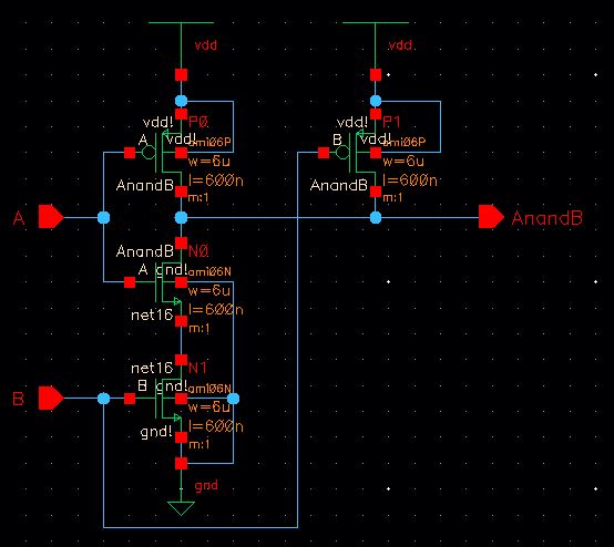
1 NAND gate using 6/0.6 NMOS and PMOSs
-
1 NOR gate using 6/0.6 NMOS and PMOSs
-
1 inverter made with a 6u/0.6 NMOS and 12u/0.6u PMOS
-
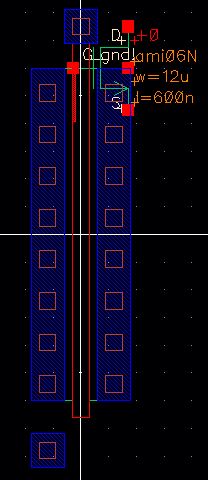
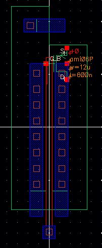
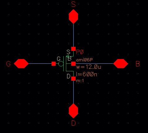
1 6u/0.6u 4-terminal PMOS transistor
-
1 6u/0.6u 4-terminal NMOS transistor
-
1 25k-10k voltage divider
-
4 (each group member's) sequence detectors that detect the
sequence 101011
Pin Connections
| Pin |
|
Component | | Considerations |
| 1 |
|
A | | - NAND
and NOR share the same A and B inputs (pins 1 and 40 - which are the
top left and right pins to on the package) to simplify connections and
reduce the number of pins needed
- each component's terminals are physically next to one another
- 25k reistor can be accessed on its own, as well as operate in the voltage divider
- each
detector shares the same clock and sequence input (pins 30 and 31) to
simplify connections and reduce the number of pins needed
|
| 2 |
AnorB |
| 3 |
NOR vdd |
| 4 |
PMOS G |
| 5 |
PMOS D |
| 6 |
PMOS B |
| 7 |
PMOS S |
| 8 |
RS detect out |
| 9 |
RS detect vdd |
| 10 |
TH detect out |
| 11 |
TH detect vdd |
| 12 |
|
| 13 |
|
| 14 |
|
| 15 |
NMOS D |
| 16 |
NMOS G |
| 17 |
NMOS S |
| 18 |
25k (out) / 10k (in) |
| 19 |
25k (in) |
| 20 |
ground |
| 21 |
TKF Detector vdd |
| 22 |
TKF buffout |
| 23 |
SM buffout |
| 24 |
|
| 25 |
|
| 26 |
SM Detector vdd |
| 27 |
|
| 28 |
|
| 29 |
|
| 30 |
detector inputs |
| 31 |
detector clks |
| 32 |
|
| 33 |
NAND vdd |
| 34 |
inverter vdd |
| 35 |
Ring Osc OUT |
| 36 |
Ring Osc VDD |
| 37 |
Inverter OUT |
| 38 |
Inverter IN |
| 39 |
AnandB |
| 40 |
B |
Testing the Chip
- Use 5V for VDD connections
- Pin 20 is common ground for all components
|
25k Resistor
- pin 18 and pin 19
- (independent of VDD and ground)
|
25k-10k Voltage Divider
- In - pin 18
- Out - pin 19
- ground - pin 20
|
NAND
- VDD - pin 33
- GND - pin 20
- A - pin 1
- B - pin 40
- A NAND B - pin 39
|
NOR
- VDD - pin 3
- GND - pin 20
- A - pin 1
- B - pin 40
- A NOR B - pin2
|
Inverter
- VDD - pin 34
- In - pin 38
- Out - pin 37
- ground - pin 20
|
Ring Oscillator |
PMOS
- G - pin 4
- D - pin 5
- B - pin 6
- S - pin 7
|
NMOS
- D - pin 15
- G - pin 16
- S - pin 17
- B - (ground) pin 20
|
Detectors - Sequential input - pin 30
- Clock signal - pin 31
- Tyler Ferreira's
- VDD - pin 21
- output - pin 22
- Tyler Huddleston's
- VDD - pin 11
- output - pin 12
- Sharyn Miyaji's
- VDD - pin 26
- output - pin 23
- Rahell Sadiq's
- VDD - pin 9
- output - pin 8
|
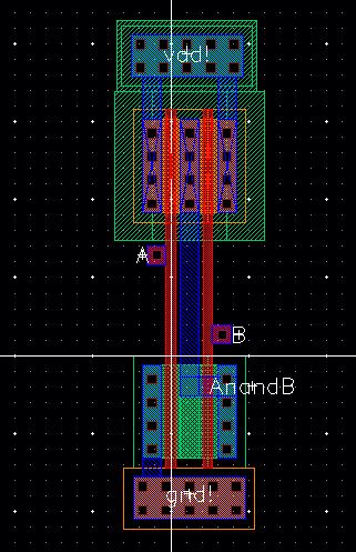
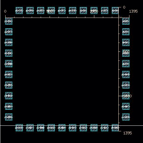
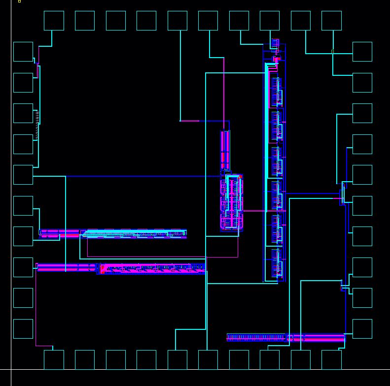
Chip Layout
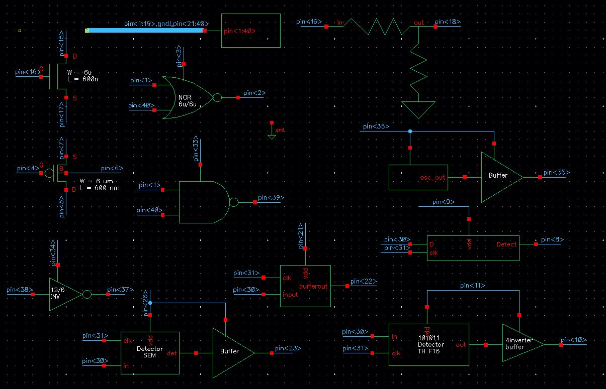 |
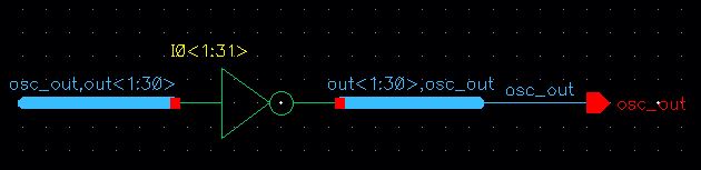
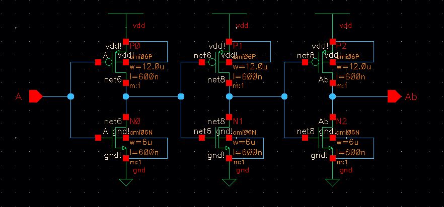
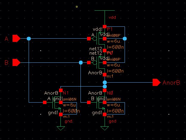
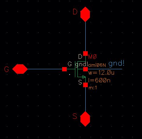
Schematic
- pin connections indicated on inputs and outputs of schematic symbols
|
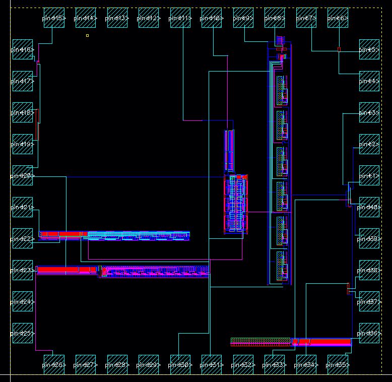 |
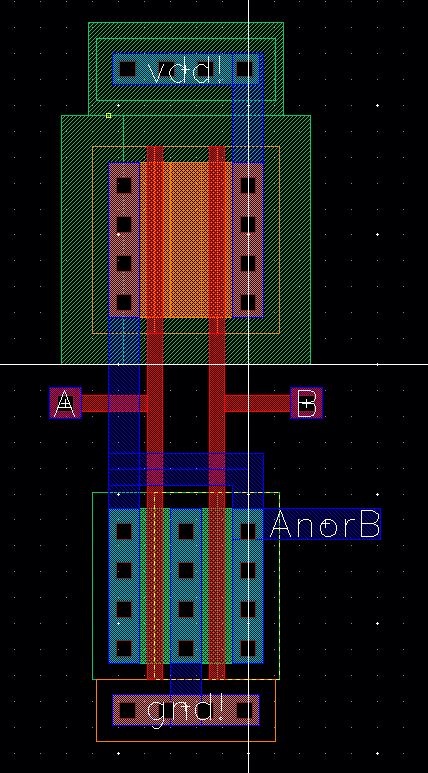
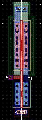
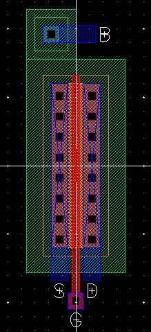
Layout
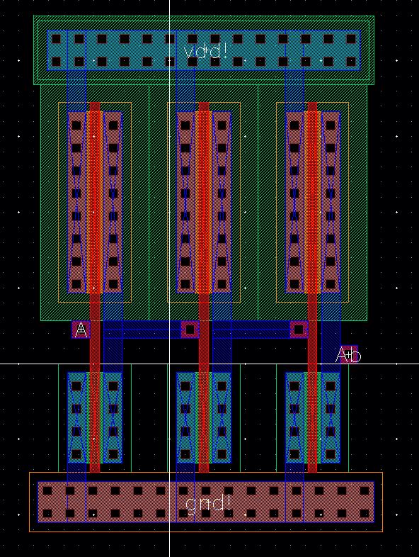
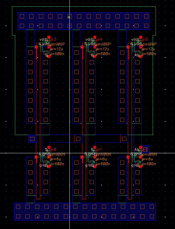
- components are laid out with buffers to the pin connections for driving capacitive loads
|
 |
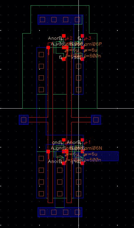
Extracted Layout |
|
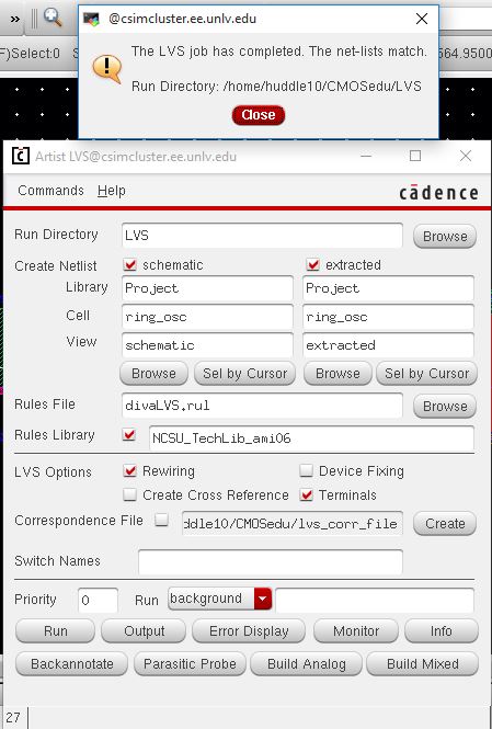
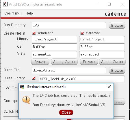
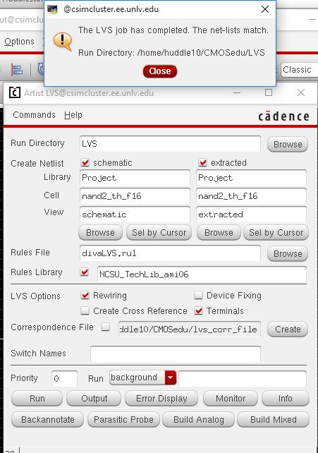
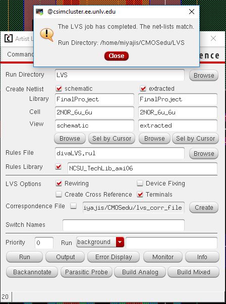
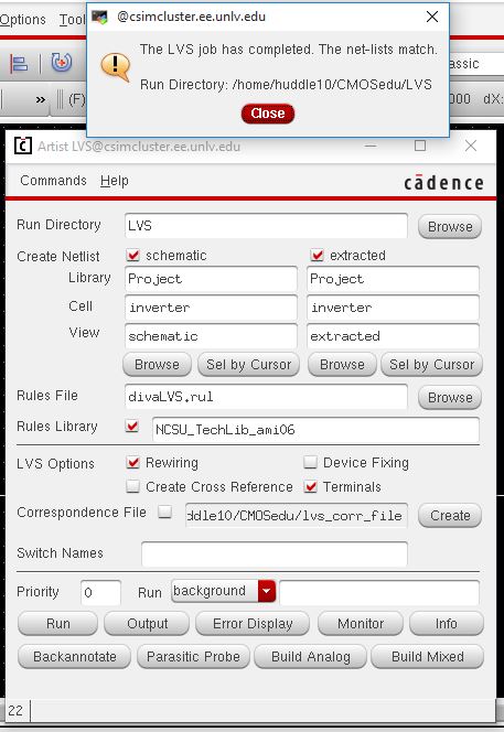
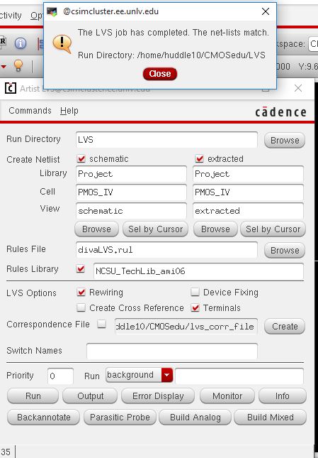
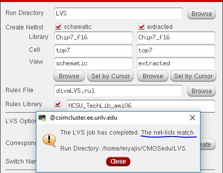
Layout LVSs |
|
|
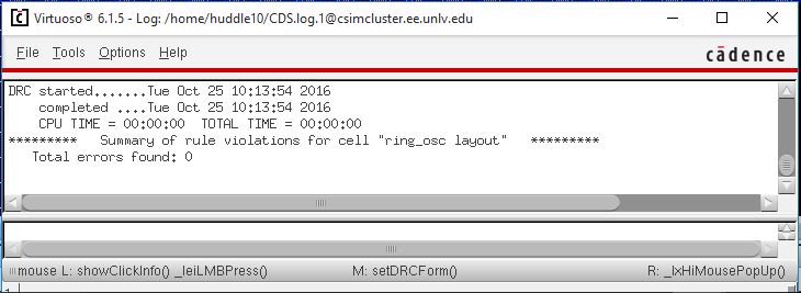
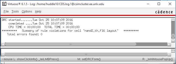
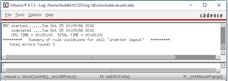
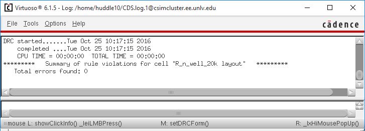
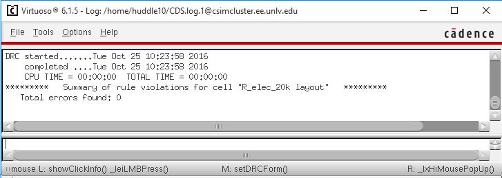
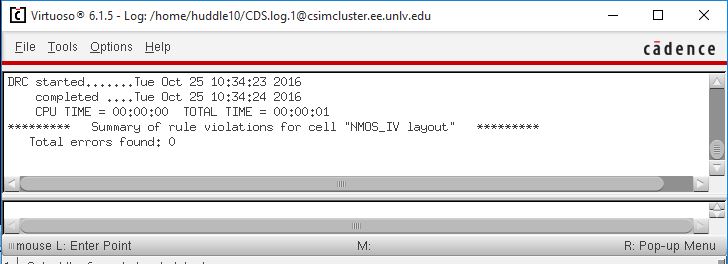
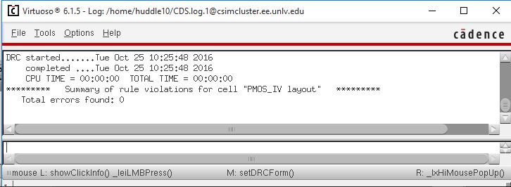
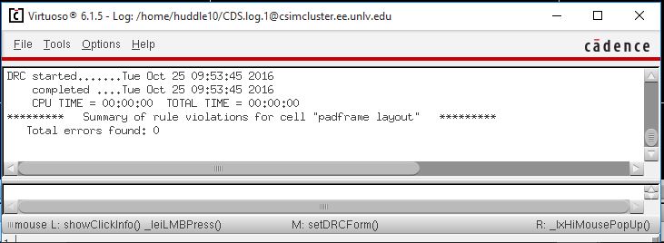
Layout DRCs |
Small Cells laid out, DRC'd, and
LVS'd
31-Stage
Oscillator:
Buffer to
drive 20pF load:
NAND
gate with 6/0.6u NMOSs and PMOSs:
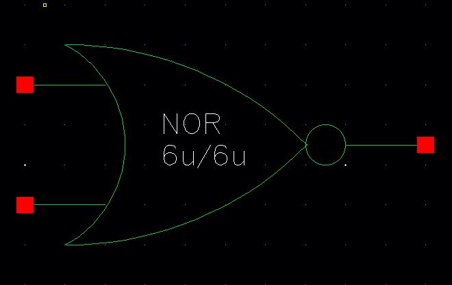
NOR gate
with 6/0.6u NMOSs and PMOSs:
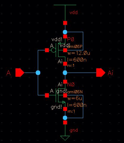
Inverter
made with a 6/0.6 NMOS and a 12/0.6 PMOS:
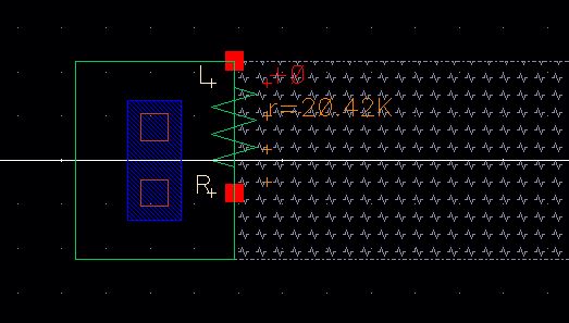
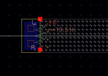
Two
20k resistors, one made using n-well and the other using hi-res poly2:
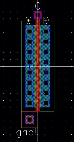
12u/0.6u
PMOS and NMOS devices:
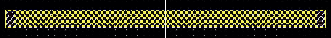
Padframe:
Return
to EE 421L Labs