Lab 4 - ECE 421L
Author: Matthew Weishaar
weishm1@unlv.nevada.edu
Date: September 15, 2021
Lab
description and goals:
Learn how NMOS and PMOS devices function and how to do layouts and schematics with them.
Prelab:
Go through Tutorial 2
Lab:
First
off we create four schematics to learn how to create schematics for
NMOS and PMOS and how the output process can vary depending on the
values of VGS/VSG and VDS/VSD.
First Schematic: ID v. VDS, VGS varies from 0-5V in 1V steps, VDS varies from 0-5V in 1mV steps, 6u/600n width-to-length


 NMOS
schematic
Simulation
NMOS
schematic
Simulation
Second Schematic: ID v. VGS, VGS varies from 0-2V in 1mV steps, VDS = 100mV, 6u/600n width-to-length


NMOS
schematic
Simulation
Third Schematic: ID v. VSD, VSG varies from 0-5V in 1V steps, VSD varies from 0-5V in 1mV steps, 12u/600n width-to-length


PMOS
schematic
Simulation
Fourth Schematic: ID v. VSG, VSG varies from 0-2V in 1mV steps, VSD = 100mV, 12u/600n width-to-length


PMOS
schematic
Simulation
Next we are laying out an NMOS device that is 6u/.6u and we will connect each terminal to probe pads:

We will create a schematic to test our layout:
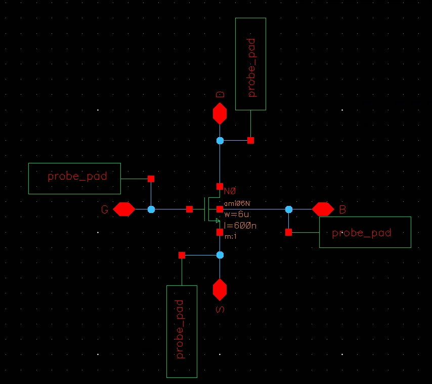
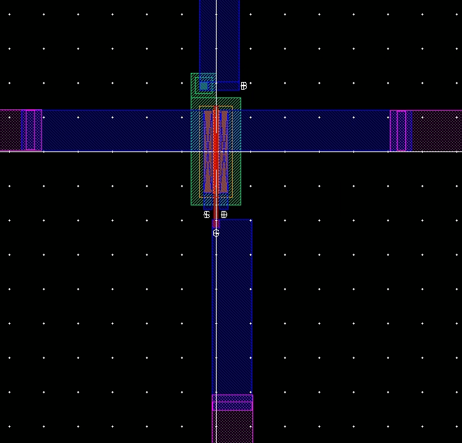
Once our layout is finished we should end up with this.


Then, as always, we DRC our layout.

Once we have passed the DRC check, we will extract our layout and run that against the schematic we created.

The netlists match so we know our layout is correct.
Lastly we will create a PMOS device that is 12u/.6u with the terminals also connected to probe pads.
Schematic:

Layout:

DRC:
LVS:

Lastly, never forget to backup your work.

Return to labs