
Lab Project - EE 421L
(ruangnol@unlv.nevada.edu)
SRAM
| SRAM Schematic |
|
| SRAM Symbol |
 |
Below are the SRAM Layout and Extracted:
| SRAM Layout | SRAM Extracted |
 |  |
Below are the SRAM DRC and LVS:


SRAM Simulation:
| SRAM Schematic |
 |
| SRAM Simulation |
 |
SRAM stores value when Row is high.
8-Bit SRAM or Word
The next step in the project is to create a 8-bit SRAM cell by combining 8 1-bit SRAM cells. This will create 1 word
| 8-bit SRAM Schematic |
 |
| 8-bit SRAM Symbol |
 |
Below are the SRAM Layout and Extracted:
| 8-bit SRAM Layout |
 |
| 8-bit SRAM Extracted |
 |
Below are the 8-bit SRAM DRC and LVS:


| 8-bit SRAM Schematic |
 |
| 8-bit SRAM Simulation |
 |
8-bit SRAM stores value when Row is high.
5 Input NAND GATE
We will create a 5 input NAND gate as a subsection of the row decoder.
This NAND gate is needed to obtain uniques addresses throughout the 32 word array.
| NAND Gate Schematic |
 |
| NAND Gate Symbol |
 |
Below are the NAND Gate Layout and Extracted:
| NAND Gate Layout | NAND Gate Extracted |
 |  |
Below are the NAND Gate DRC and LVS:


| NAND Gate Schematic |
 |
| NAND Gate Simulation |
 |
From the results, we can see that as the gate runs "high" all outputs will be "0".
5 Input AND GATE
Our NAND gate but with an inverter at the end.
| AND Gate Schematic |
 |
| AND Gate Symbol |
 |
Below are the NAND Gate Layout and Extracted:
| AND Gate Layout |
 |
| AND Gate Extracted |
 |
Below are the AND Gate DRC and LVS:


| AND Gate Schematic |
 |
| AND Gate Simulation |
 |
From the results, we can see that as the gate runs "high" all outputs will be "1"
32 Word Array
Next we instantiate th 8-Bit word cell or SRAM eight times to create a 32 Word Array.
The 32 Word array is going to be our memory storage for the Register File. Each row can be read by using a row decoder to turn on that row.
| 32 Word Array Schematic |
 |
| 32 Word Array Symbol |
 |
Below are the 32 Word Array Layout and Extracted:
| 32 Word Array Layout | 32 Word Array Extracted |
 |  |

Below are the 32 Word Array DRC and LVS:


32 Word Array Simulation:
| 32 Word Array Schematic |
 |
| 32 Word Array Simulation |
 |
32 Word Array stores value when Row is high.
Row Decoder
A large component of the register file is the row decoder.
The row decoder will determine which of the 8-bit word cell will be turned on.
There are 32 possible addresses to choose from.
Address:
| Row | 5-Bit Address |
| 0 | 00000 |
| 1 | 00001 |
| 2 | 00010 |
| 3 | 00011 |
| 4 | 00100 |
| 5 | 00101 |
| 6 | 00110 |
| 7 | 00111 |
| 8 | 01000 |
| 9 | 01001 |
| 10 | 01010 |
| 11 | 01011 |
| 12 | 01100 |
| 13 | 01101 |
| 14 | 01110 |
| 15 | 01111 |
| 16 | 10000 |
| 17 | 10001 |
| 18 | 10010 |
| 19 | 10011 |
| 20 | 10100 |
| 21 | 10101 |
| 22 | 10110 |
| 23 | 10111 |
| 24 | 11000 |
| 25 | 11001 |
| 26 | 11010 |
| 27 | 11011 |
| 28 | 11100 |
| 29 | 11101 |
| 30 | 11110 |
| 31 | 11111 |
| Row Decoder Schematic |
 |
| Row Decoder Symbol |
 |
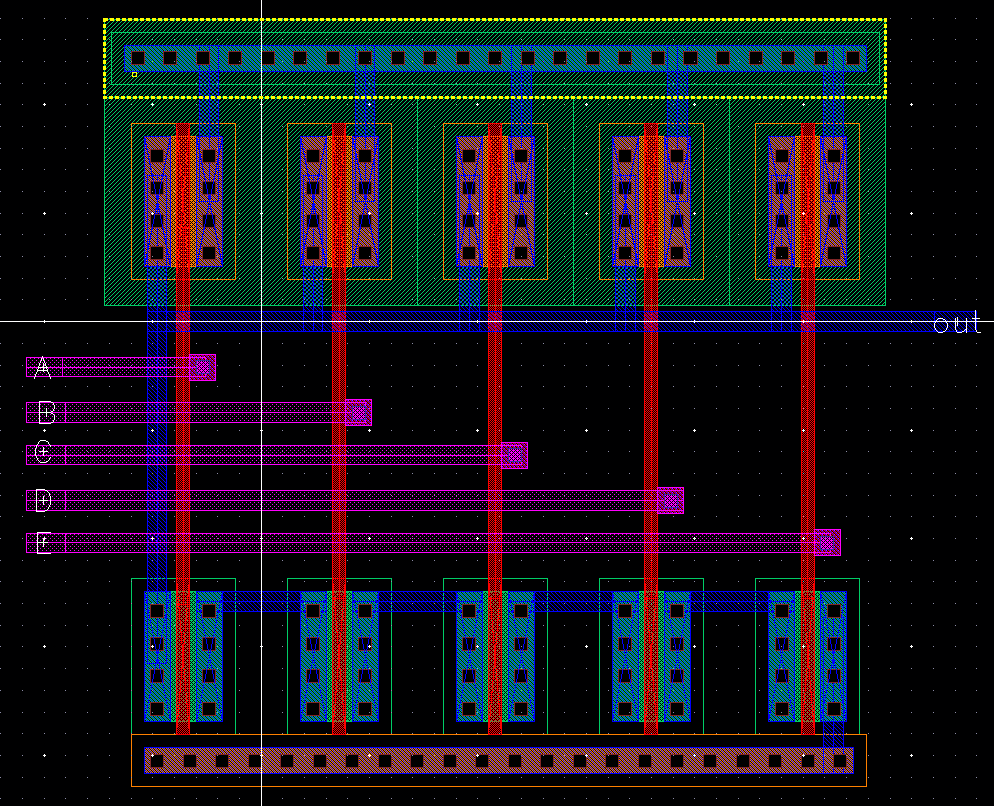
Below are the Row Decoder Layout and Extracted:
| Row Decoder Layout | Row Decoder Extracted |
 |  |
| Row Decoder Top |
 |
| Row Decoder Bottom |
 |
Below are the Row Decoder DRC and LVS:


| Row Decoder Schematic |
 |
| Row Decoder Simulation |
 |
When the inputs of A,B,C,D,E is "1" then the address then Row 31 turns on.
Register File
The Register file is the combination of all the components worked on this project. The Read/Write input signal is added to determine were the RF reads "1" or writes "0". This will also separate the outputs by running it through NMOS's.
| Register File Schematic |
 |
| Register File Symbol |
 |
Below are the Register File Layout and Extracted:
| Register File Layout | Register File Extracted |
 |  |
Below are the Register File DRC and LVS:


Register File Simulation:
| Register File Schematic |
 |
| Register File Simulation |
 |

Conclusions
To make this simulation more cleaner, the original design would need capacitors throughout the circuit to properly power each components without delay.
The simulation must have a high enough pulse width to be able to read and write the data inputs from the row decoder.
The Design is functional to its basic operation, but further improvements can be made to better the outcome. (Increasing power distribution).
Project Files are Located Here
Return to EE 421L Labs