Lab 7 - EE 421L
Authored
by Ricardo Rodriguez
UNLV E-mail: rodrir15@unlv.nevada.edu
November 3, 2021
Prelab Work:
- Backed up all work presented in lab by zipping the FTP folder and emailing the new file to myself
- Tutorial 5
 A ring oscillator without the use of arrays/buses
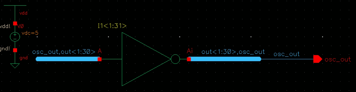
 A ring oscillator with the use of arrays/buses
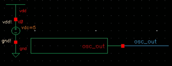
Symbol and schematic for simulation
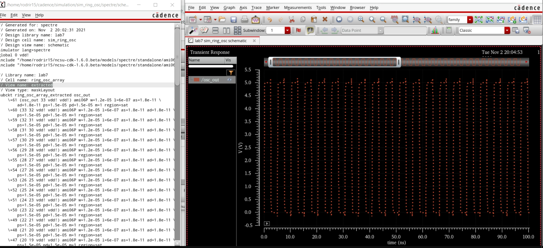
Simulation Results
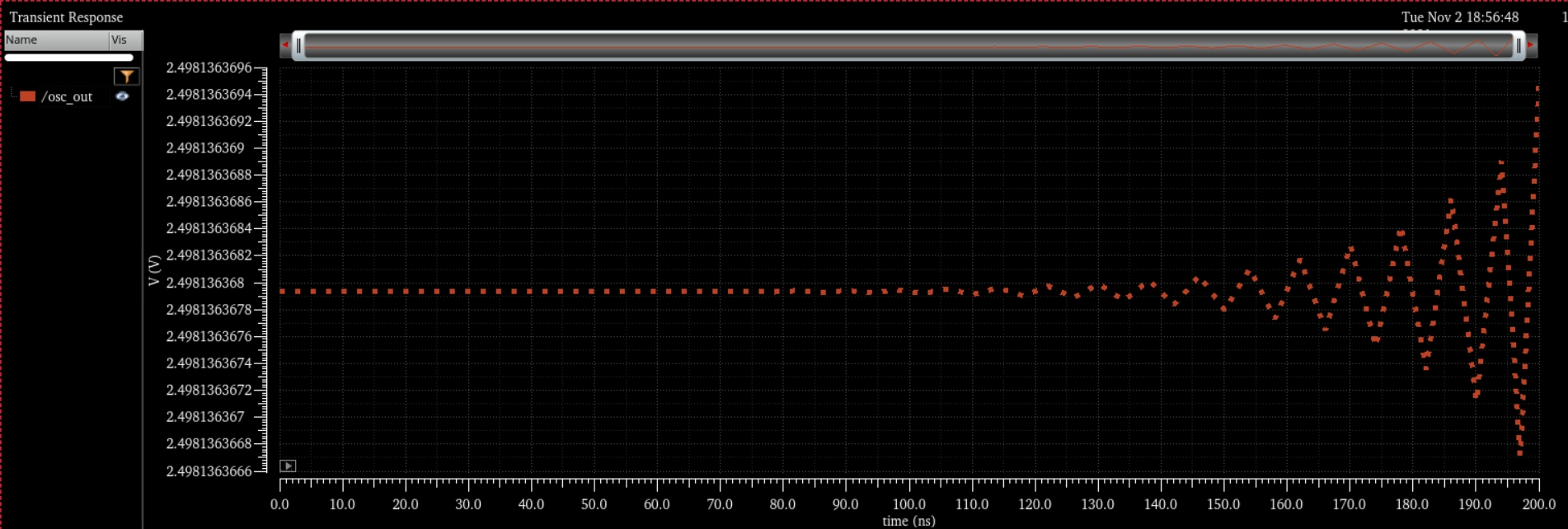
Simulation of
the ring oscillator without using initial conditions
Simulation of
the ring oscillator using initial conditions (output/input is 0)

We can add our inital condition by going to Simulations > Convergence Aids > Initial Conditions

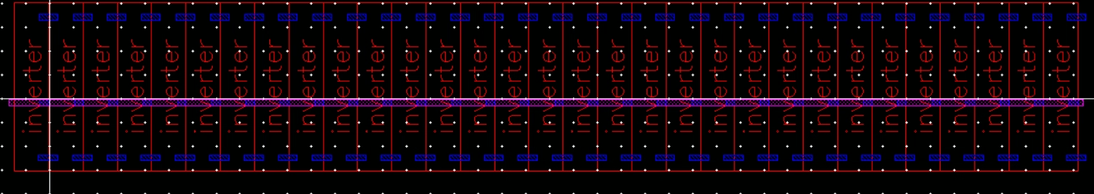
Now, to create the layout of the ring oscillator
We
connect 2 inverters together and then delete the 2nd inverter to copy
the remains and make it easier to create 31 stages


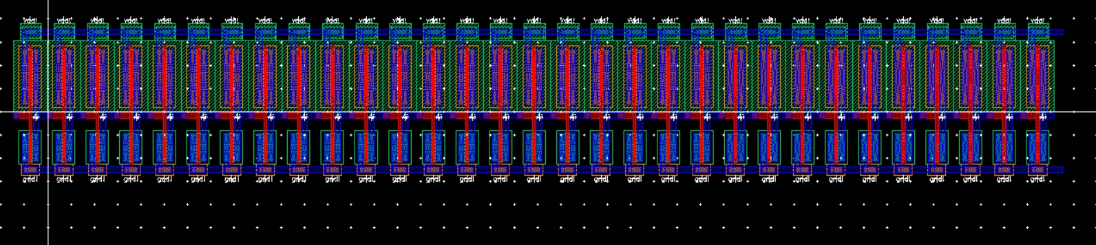
We can then connect our output to our input to create a feedback loop by connecting them to Metal2 by via
and
then we can connect our pins, but our LVS will fail as the schematic
does not have a pin for osc_out, so we have to add it in


If we LVS again, we will see that it matches and we can run the simulation off of our extraction

Lab Work:
For
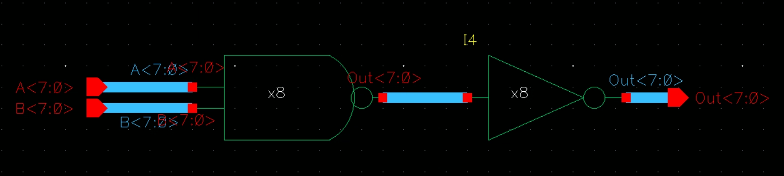
the lab we create a 4 bit inverter, an 8 bit inverter, OR, NOR, AND,
NAND gates. This is done by the use of buses rather than creating many
instances of gates
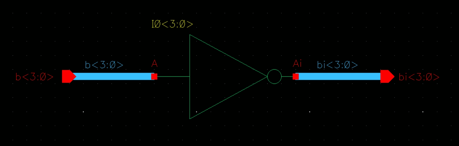
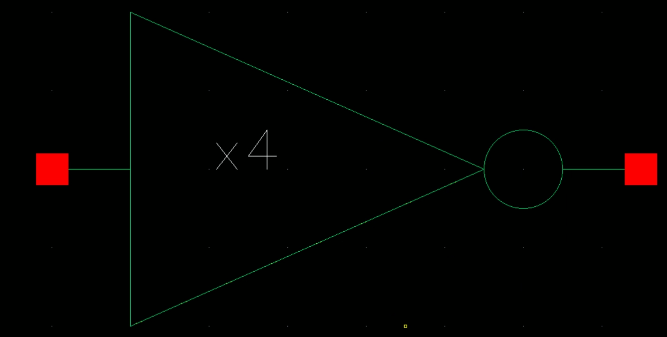
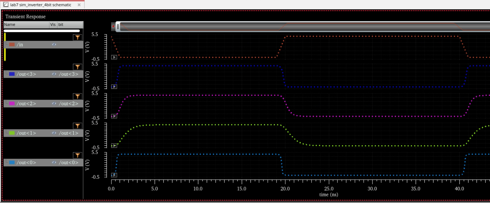
4 Bit Inverter:
Schematic
Symbol
Simulation Schematic and Sims

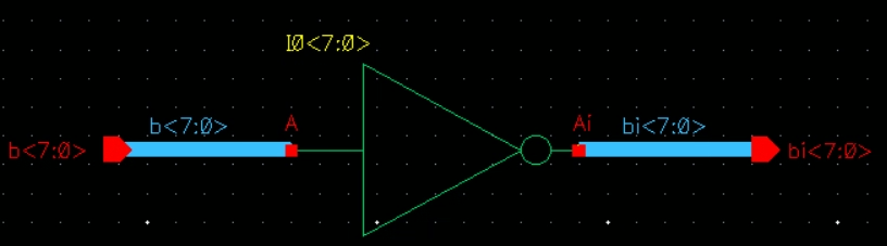
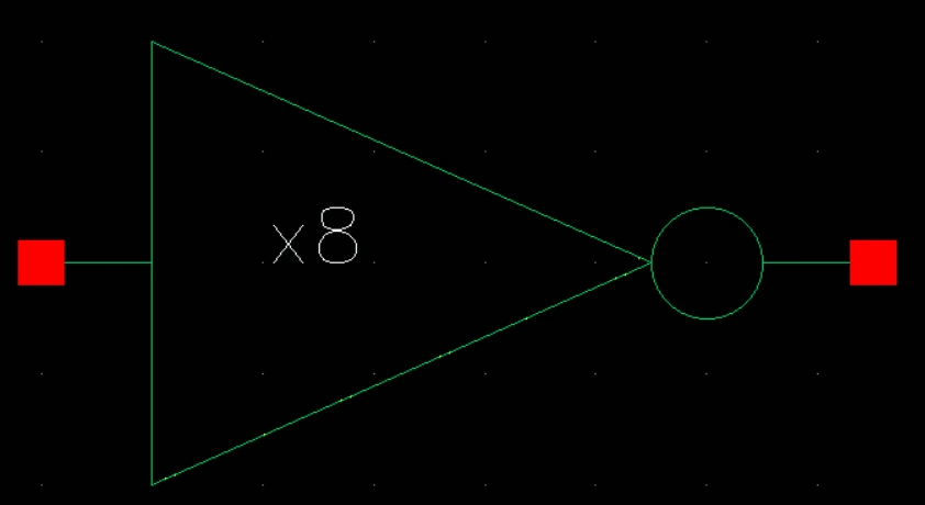
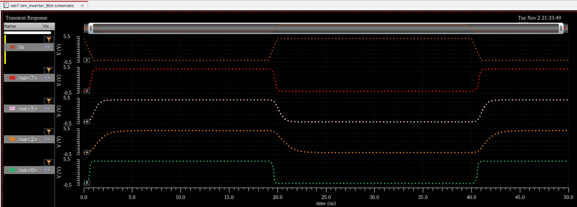
8 Bit Inverter:
Schematic
Symbol
Simulation Schematic and Sims

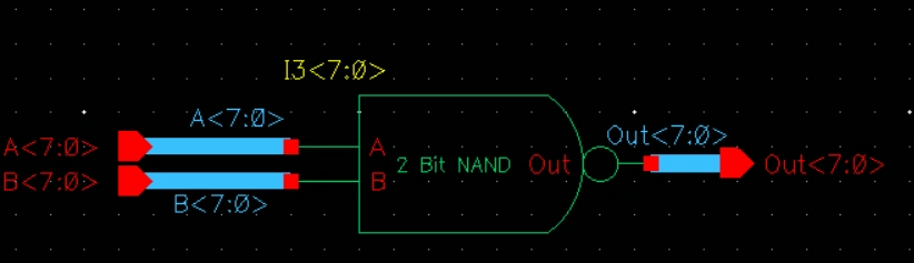
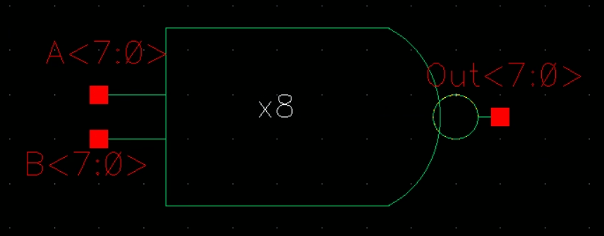
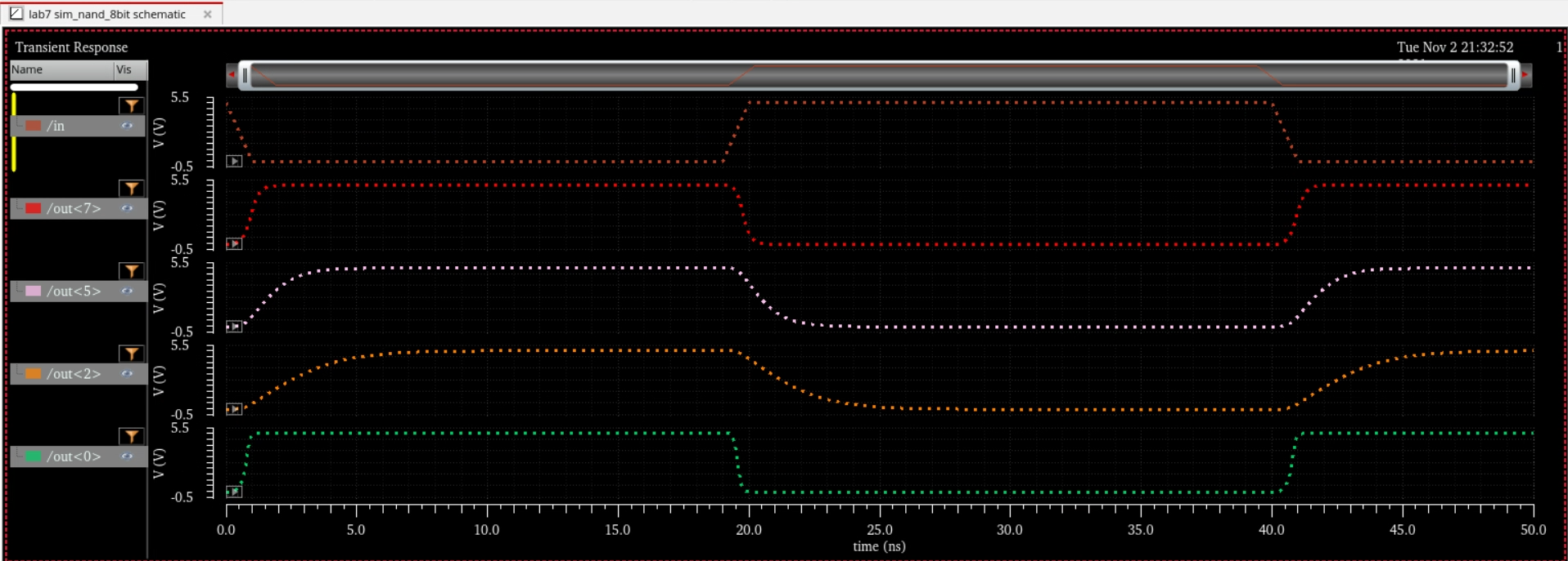
8 Bit NAND:
Schematic
Symbol
Simulation Schematic and Sims

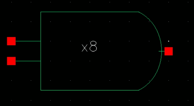
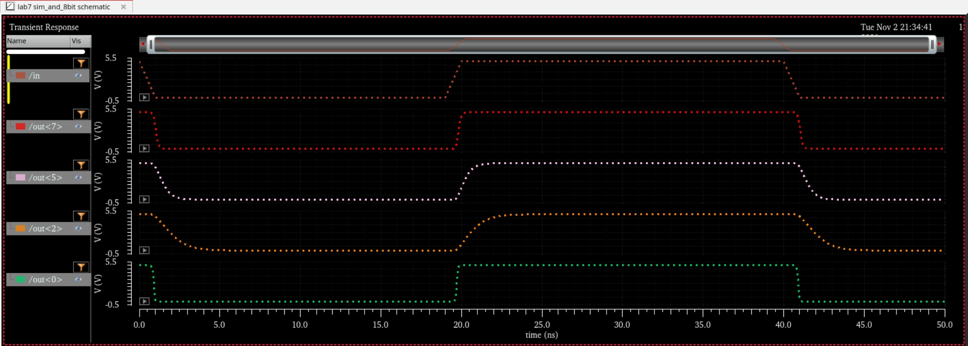
8 Bit AND:
Schematic
Symbol
Simulation Schematic and Sims

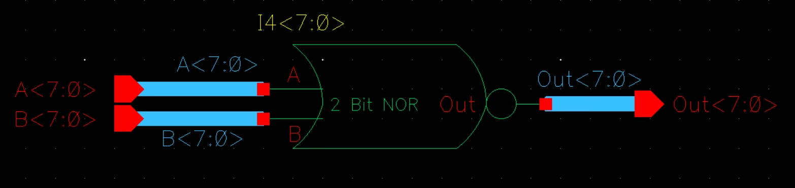
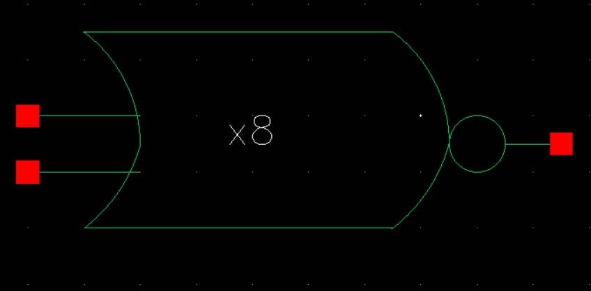
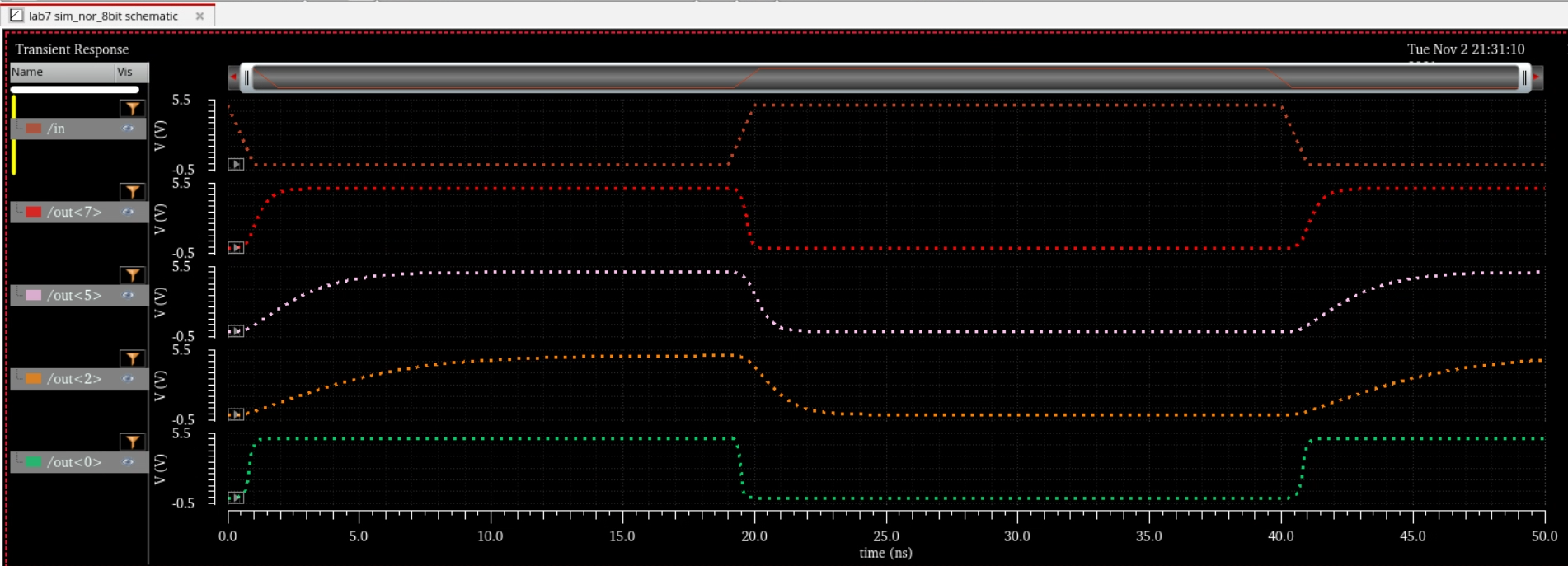
8 Bit NOR:
Schematic
Symbol
Simulation Schematic and Sims

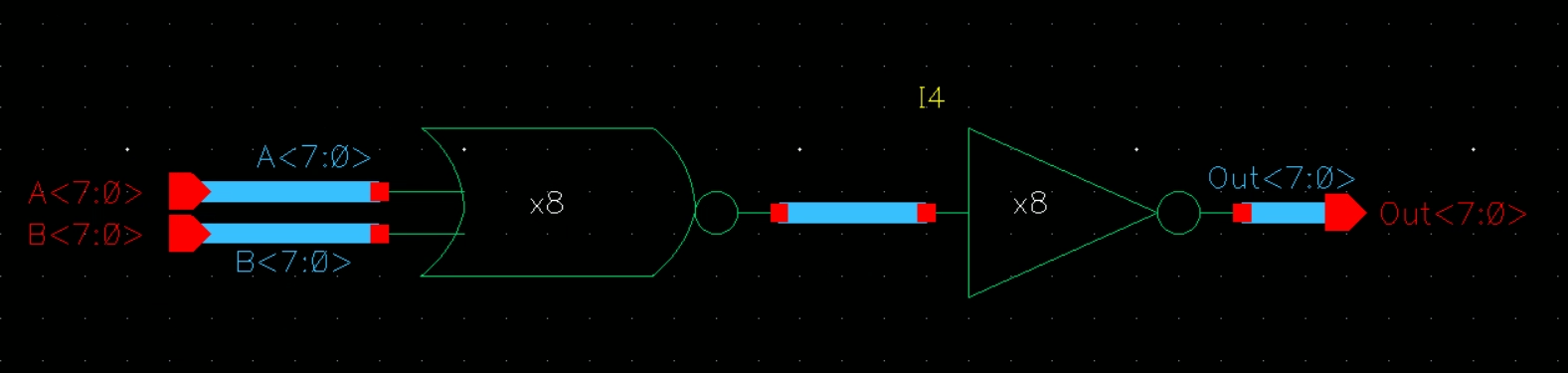
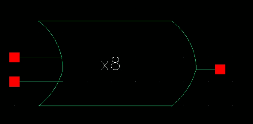
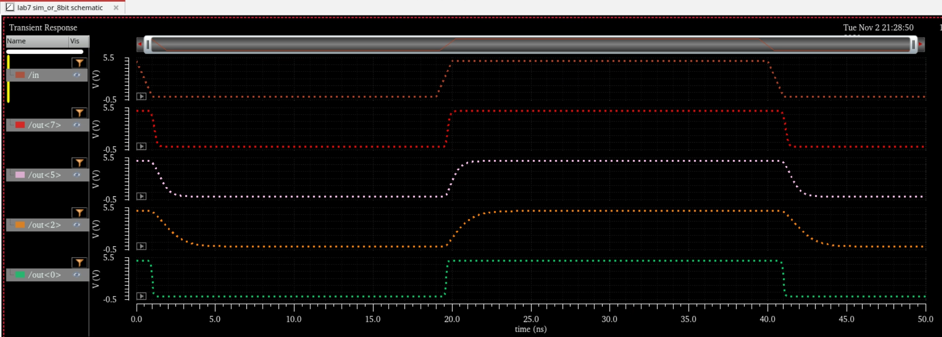
8 Bit OR:
Schematic
Symbol
Simulation Schematic and Sims

Next,
we had to work on a MUX. A MUX allows us to choose an input based off
of our selection input. It maintains the equation Z = A*S + B*Si
A DEMUX works in the opposite way. Based on our input, (z in this case) we can choose either A or B based off of our S and Si
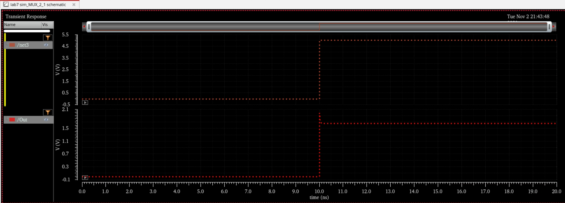
Operation of a MUX.
Schematic to simulate the MUX
Simulation of the MUX

Now we create an 8bit MUX like the following
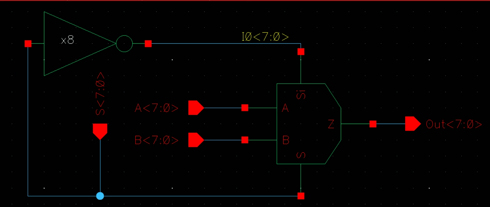
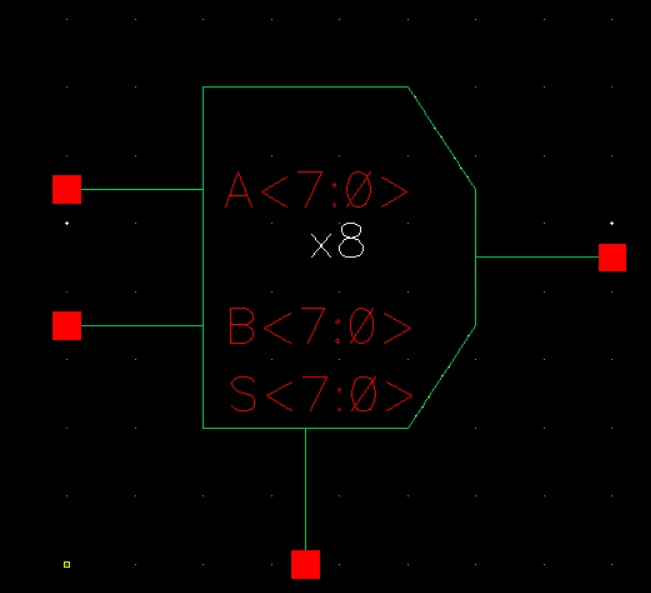
with this symbol (our Si is built-in)
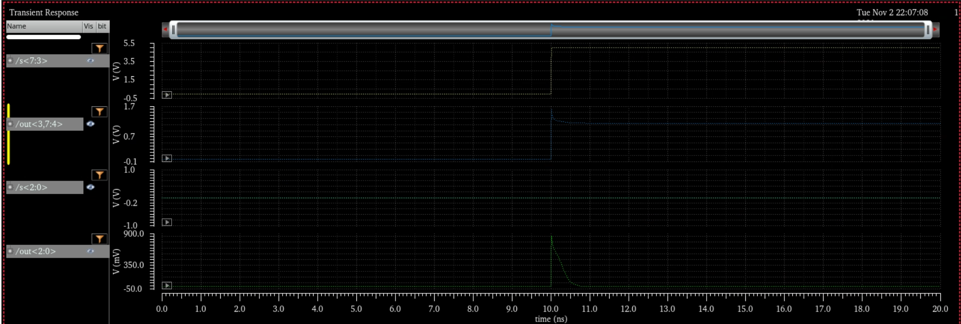
We can simulate our 8 bit mux like this

The next part of the lab is to create an 8bit adder. We do this by starting from the beginning
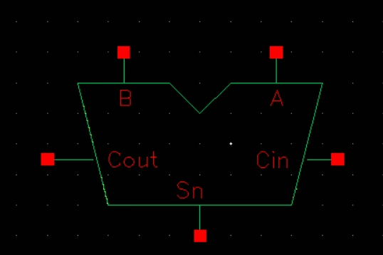
Schematic for a 1bit adder
Symbol for the full adder

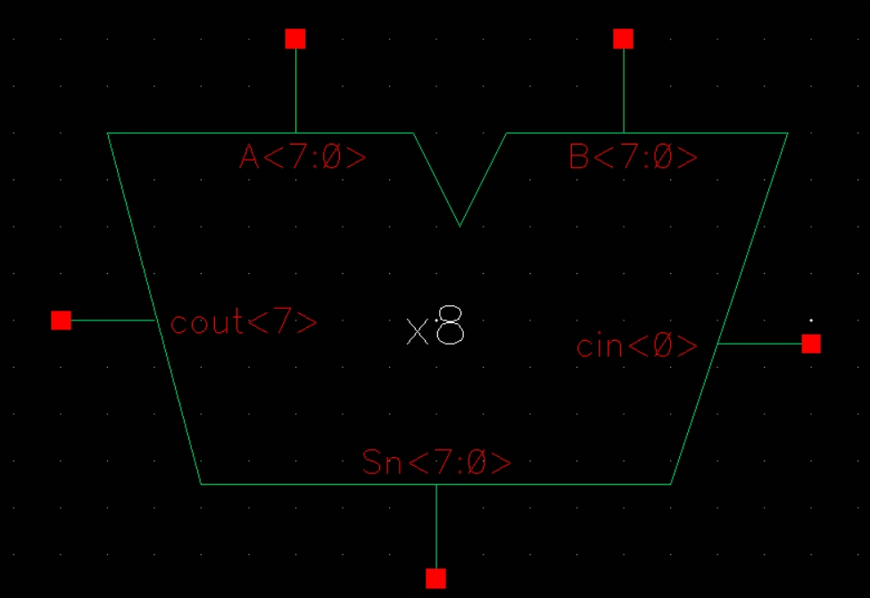
An 8 bit
adder using buses and arrays
Symbol for the
8bit full adder
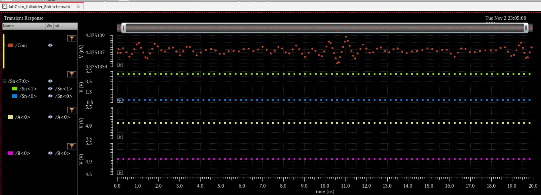
Simulating the adder by adding
A:00000001 and
B:00000001
Our output is
Cout:0 Sn:00000010
Return to my labs
Return to student labs