Lab 4 - ECE
421L
Prelab:
For this prelab, I shall be
demonstrating the different tasks given for Tutorial 2:
In tutorial 2, we needed to create a
layout and simulate the IV curves of a PMOS and NMOS device:
Here I have already unzipped the
following Tutorial and have created a new cell view for the prelab:

From creating an instance -> NCSU_Analog_Parts -> N_Transistors -> nmos:

From the following picture, I have
given the parameters in which:
W = 6u
L = 600n
For which then give each pin a label
for the corresponding terminals.
G = Gate
D = Drain
S = Source
gnd! = global
ground
Now we save, then create a symbol for
the given schematic:
Create -> Cell View-> From Cell
View

To demonstrate the behavior of the
created symbol of the NMOS, a simulation is given:
First, we must launch ADE L ->
Setup-> Model Libraries:

![]()

Now we select our output variables we
want to run a DC analysis on:
Outputs -> To be
Plotted -> Select on Schematic, and click on the “D” pin

We then proceed to the following: ADE->Tools->Parametric
Analysis
Add variables = VGS
From = 0
To = 5
Step Mode = Linear Steps
Step Size = 1
Once the set up is finished, we
proceed by clicking on the Green Play Button:

Final Simulation Results:

Layout of the NMOS:
Now we create a new layout from the
given schematic and create our new instance of the NMOS:
*NOTE*: before attempting new layout
make sure the following setup for your display are the following…

This will make the process much easier
in getting the layout look we are going for.
We now have the following:

Following the layout, we then Add a ptap:

Add poly in the mix as well as our
metal1, we then have the new look:
Proceeding any Further, we always must
DRC to check if we have any errors, Verify -> DRC


Following the new layout, we then add
our pins.

Now it’s time to extract the layout
Verify -> Extract.
We then have the following extracted
layout:

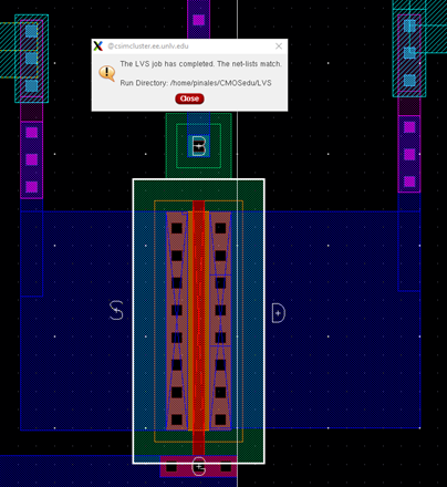
From the extracted layout, Now run a
LVS (Verify -> LVS) to verify the extracted and schematic work.

Once passed, we then proceed back to
the schematic so we can now display the results for the given variables through
simulation result:

ID v. VDS
PMOS Schematic/Layouts:
Now to the next task given, we proceed
by forming the schematic of the PMOS:
Create instance (Keybind
i) -> pmos4
component (With W=12μ and L=600n):

Always Check and Save!
![]()
Then once again, Create
a symbol (Create - > Cellview -> From Cell View):

Now, to create a new layout for the
PMOS:
Similar to the NMOS layout
except this time we will be Adding a Ntap from the
following location Keybind I -> NCSU_Techlib_ami06 -> ntap
Final Layout Result:

Now, Extract and run the LVS for the files:


Success! (If everything did pass) we
now proceed to demonstrating the given schematics through simulations:
LAB 4:
Experiment 1:

ID. v VDS of an NMOS device for VGS varying from 0 to 5 V in 1 V steps while VDS varies from 0 to 5 V in 1 mV steps.
Experiment 2:
![]()


A schematic for simulating ID v. VGS of an NMOS
device for VDS = 100 mV where VGS varies from 0 to 2 V in 1 mV steps.
Experiment 3:

Proceed the same as NMOS simulations(ADE L -> Setup
-> Model Libraries) with the given parameters
![]()
![]()


ID v. VSD (note VSD not VDS) of a PMOS
device for VSG (not VGS) varying from 0 to 5 V in 1 V steps while VSD varies
from 0 to 5 V in 1 mV steps
Experiment 4:


ID v. VSG of a PMOS device for VSD = 100 mV
where VSG varies from 0 to 2 V in 1 mV steps.
Experiment 5:
According to the rules of the MOSIS
Layout, a bonding pad’s layout should be laid out by the given parameters:
Center layer: Probe pad (Glass) approx.
= 20.4um x 20.4um
Topmost layer: Metal3
Pad/Metal Overlap:
greater than 6μm
Total measurement of
bonding pad: 16.35μm
Total measurement of
Metal3 layer: 32.7μmx32.7μm
Creating the probe pad:

Schematic of Probe
pad:

Symbol (Generated by schematic->create->cell
view->From Cell view):

NMOS Schematic using Probe pad:

Now that the check passes the NMOS
schematic with 4 probes, we move on to the layout.
NMOS Layout:
Before starting, look for your display
options (keybind e) and set the following so the
layout can run a bit smoother:
![]()

![]()
![]()


After using the probe pads created in
the beginning, we now have the finished result with all our layers in place and
passing a DRC and LVS!
PMOS layout with Probe Pads:
Since we already have something similar
already made for the PMOS from tutorial 2, we’ll be using that layout on top of
tweaking the schematic of the new PMOS.

Now that everything is checked and
clear to go, we layout the PMOS with the probe pads we have made.
Final Layout for PMOS:


Now that we have passed our LVS check
we finalize this lab re-running experiments so check the extracted layouts:
NMOS:


PMOS:


Done.