
Lab 1 - ECE 421L
NCSU Cadence Design Kit (CDK) version 1.6.0 beta. Which can be located at http://www.eda.ncsu.edu/wiki/NCSU_CDK
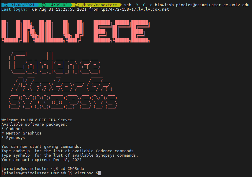
Then once all that is sorted out i was able to proceed with ssh into the csimcluster server by simplying using mobaxterminal

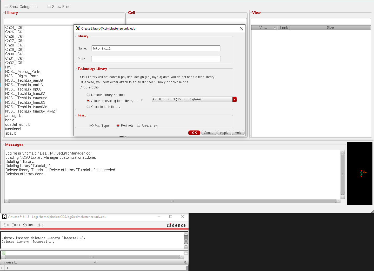
Next, We proceeded on to the initial set-up involving cadence. Here we created a library(Library Manager, File -> New -> Library) that attached our existing tech library that we had unzipped from past given zip files (NCSU Cadence Design Kit (CDK) version 1.6.0 beta). Also had to make sure that whatever library that was being created was attached to AMI 0.60u C5N process:
As well as defining the newly created library back into our .cds.lib: DEFINE Ch1_IC61 $HOME/CMOSedu/Ch1_IC61
Once the library has been created, we first start with our give task, which is to create a schematic view of our circuit:
given details: Library Manager and then the menu items File -> New -> Cell View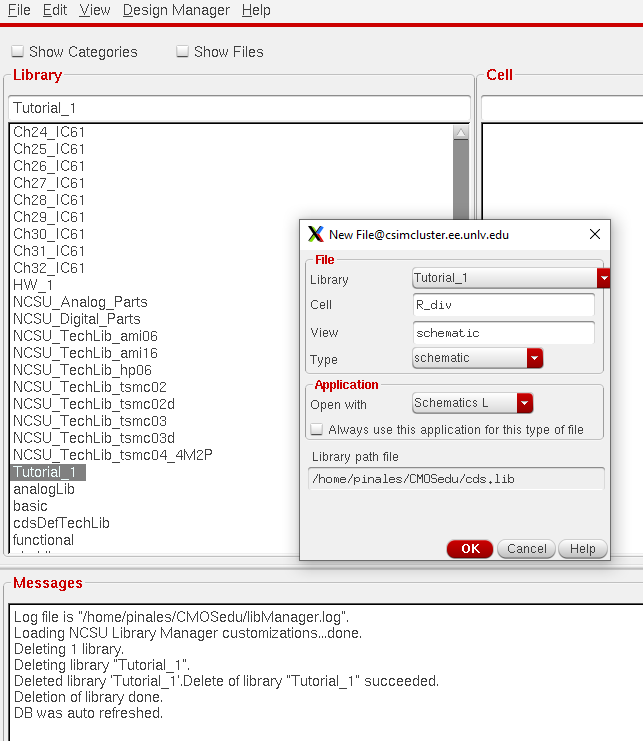
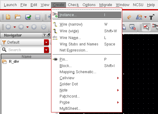
Once the schematic has been created, we start to add components to our circuit schematics:
Given Details:
Create -> Instance
Shortcut: just pressing the Bindkey i
For this circuit, we were given the task to create a voltage divder with given parameters (2 - 10k resistors):
To obtain the first component on our list we will initiated this action by using Bindkey i, then by browing our library for NCSU_ANALOG_PARTS -> R_L_C -> res

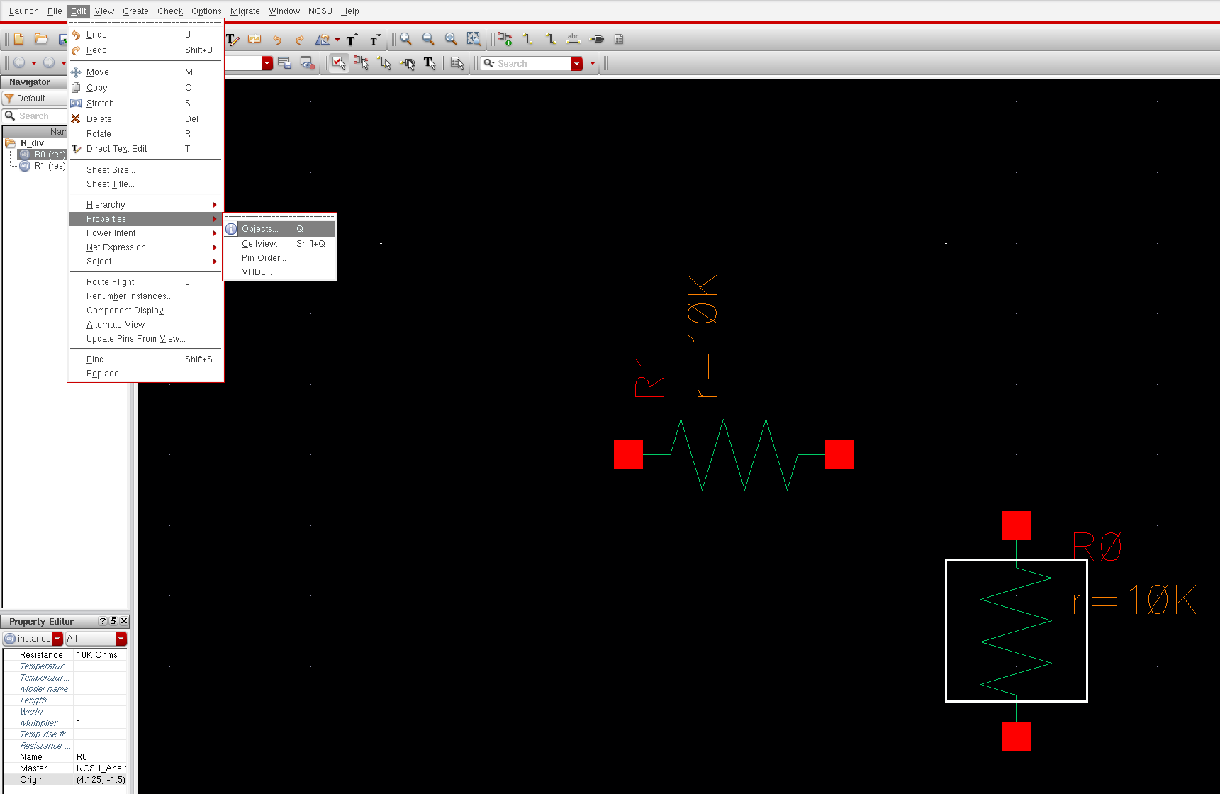
Once we've grabbed our desired amount of components, We then edit the given resistance for whatever desired resistance we want. For this example we input 10k for our OHMs
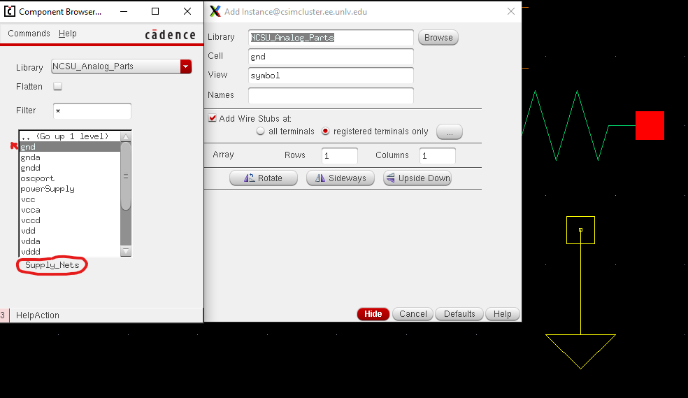
Once we're done with our resistors, we now lead towards the ground component:
Bind i -> Supply_nets -> gnd
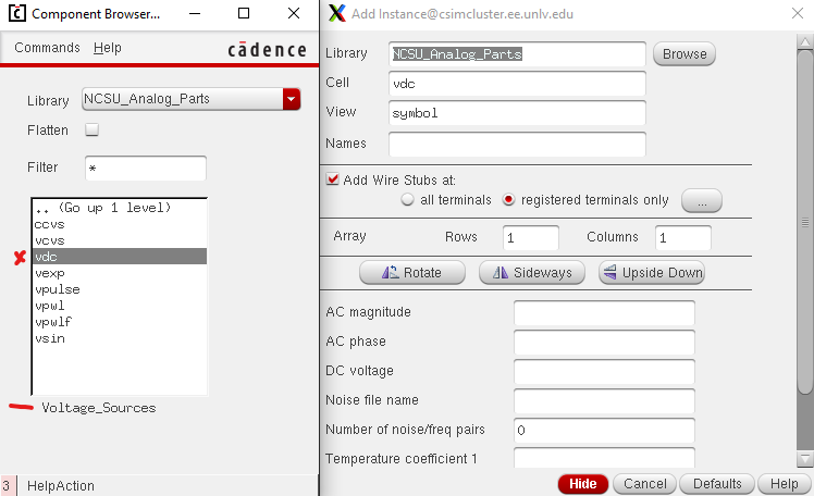
Proceeding even further, we then grab our 1-VDC source from:
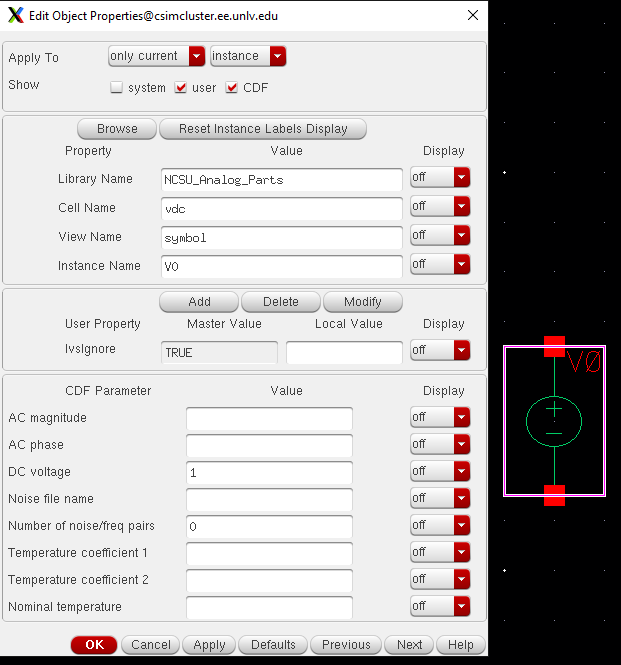
Bind i -> Voltage sources -> vdc; we can edit the parameters the same way we did our resistors.
Select component -> Bindkey q -> Desired parameters
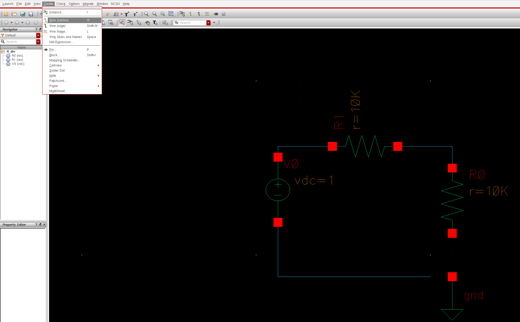
Once all components are gathered, we then proceed to the following to allow connectivity for our components (make connections with wires):
Create -> Wire or Bindkey W; Connect to ends to create a closed circuit
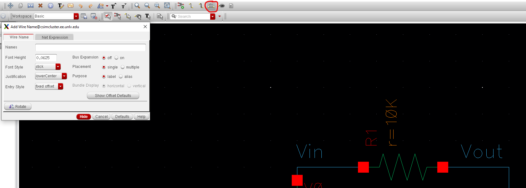
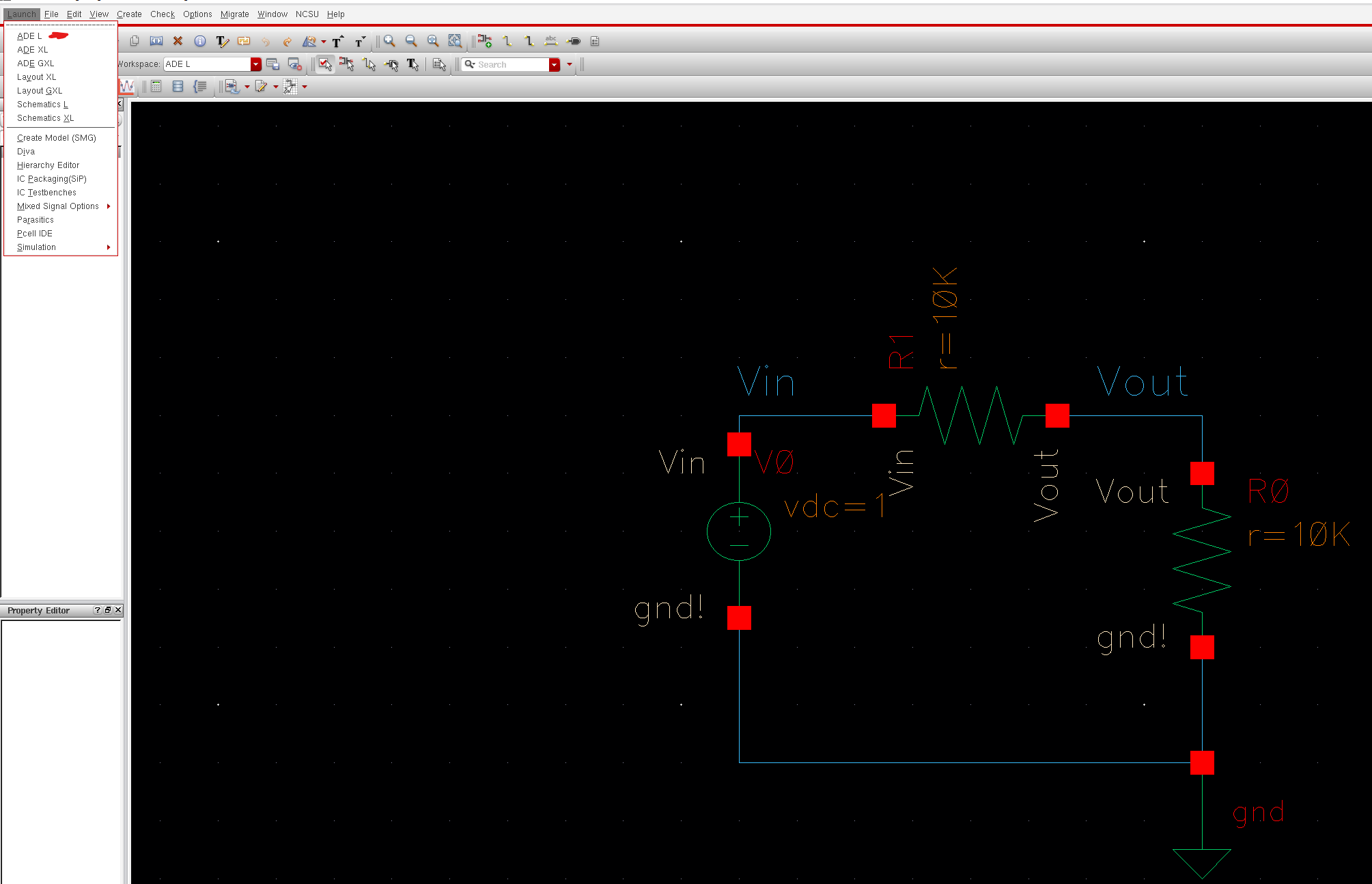
Once circuit is complete, we then can help ourselves out and label our Vin and Vout sources:
By wire symbol, there is another wire labeled with "abc" on top of it (as seen on image).
We then select which wire we want to label.
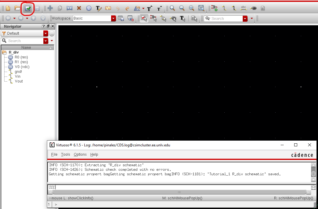
Next, we check if our circuit through simulation but first we must hit the "Check to Save" to make sure there isn't anything wrong with our connectivity of the circuit.
If the schematic has not failed during the initial check, we then simulate with Spectre (Cadence’s SPICE simulator):
go to the menu -> Launch -> ADE L
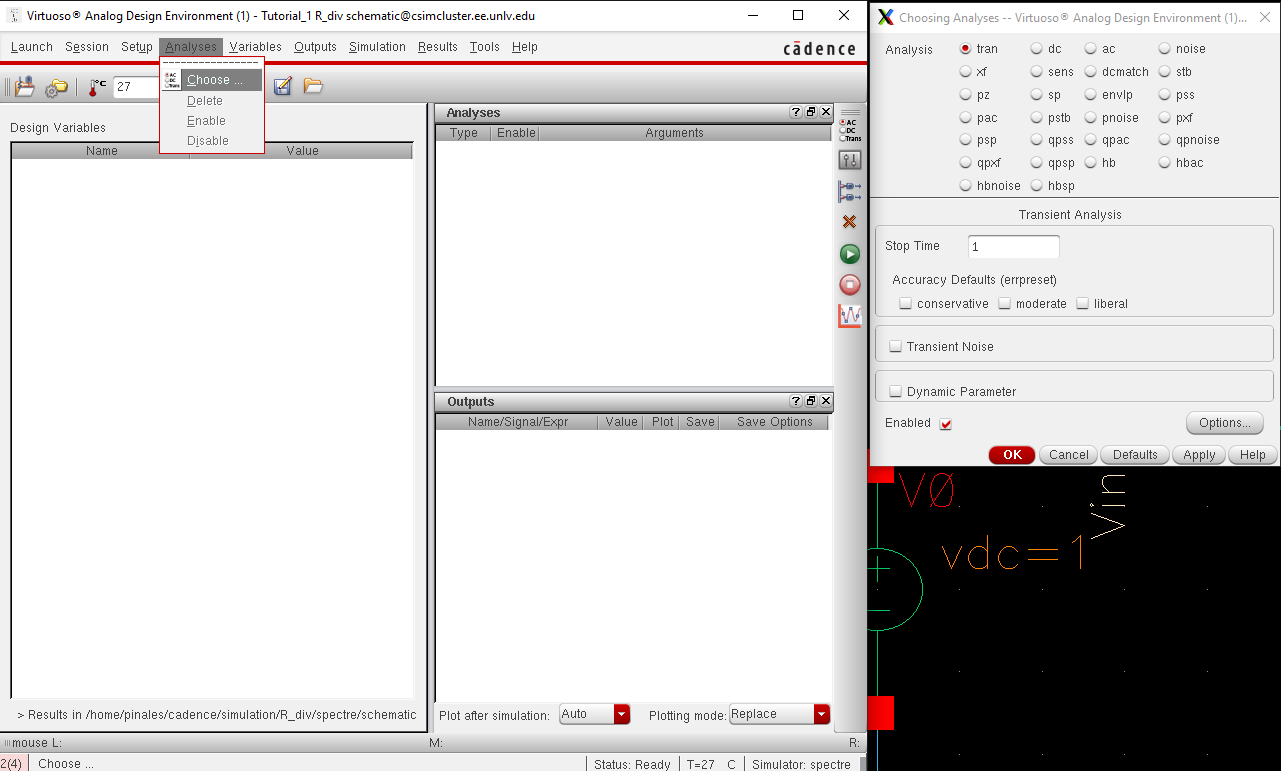
Prior to all this a helpful tip would be to have our simulator setup -> Simulator -> Spectre. This is how the setup for the entire Lab will be. Once completed we then can choose what we want to analyze in our circuit.
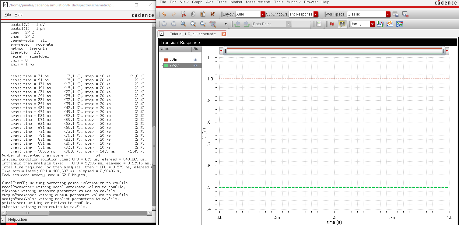
For this circuit we will be performing a Transiant analysis:
Analyses -> Choose and select a transient analysis (tran), a stop time of 1 second, and Enabled
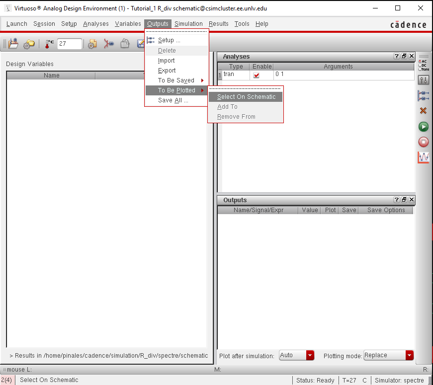
We then proceed to check which signals we want out of the circuit:
Outputs -> To be plotted -> Select on schematic.
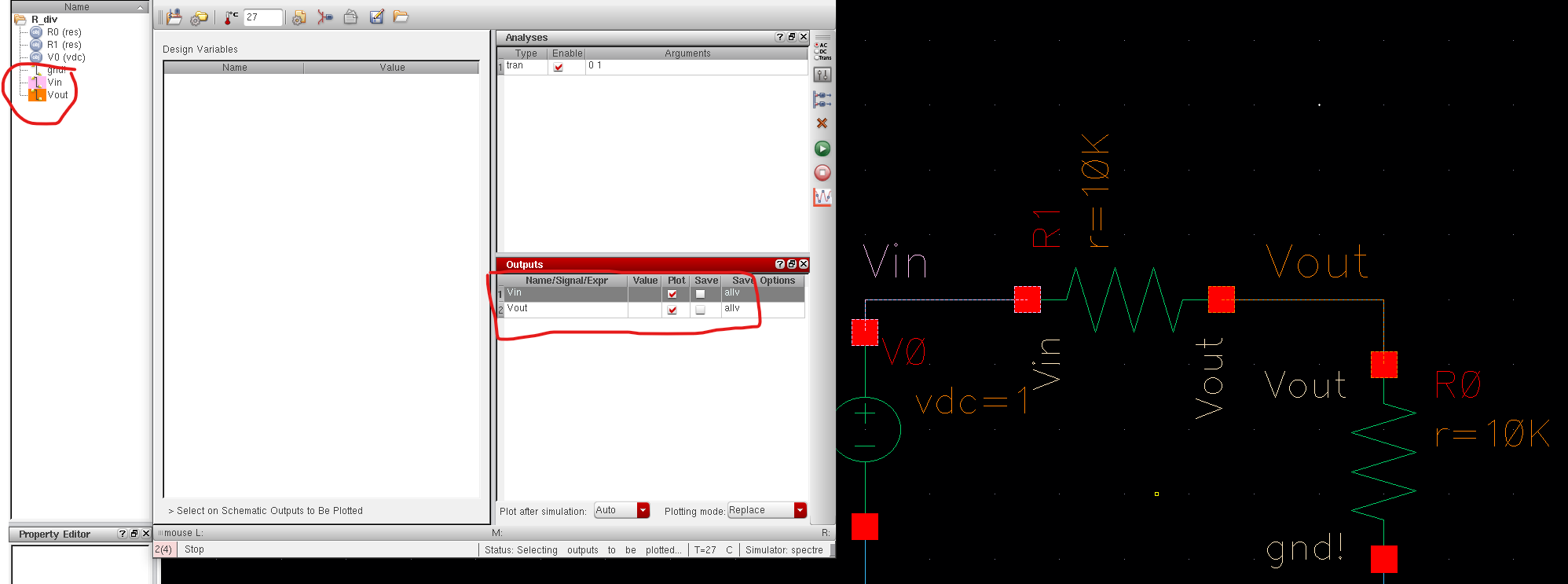
For this we shall be using the Vin and Vout signals:
Verify signals are selected though either the Name box in the schematic or By the given signals in the Output window in the Analysis page.
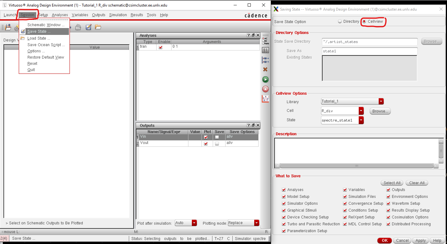
Now, if everything looks good, we then proceed to save our state (safety measures), then have it selected to cellview then select OK.
If everything works and checks out fine, you should be given a Output page of the given anaylsis response. For this example we have a Transient Response.
For Back-up Purposes: