Lab 2 - ECE 421L
Created and edited by Michael Parker
Email : parkem3@unlv.nevada.edu
Last updated : September 8 2021
Pre-Lab
- Download Lab2.zip
- Upload the contents to your CMOSedu directory.
- Define its library.
- Simulate the ADC - DAC circuit.
Lab Overview
During this lab I drafted a schematic for a 10 bit DAC based off of figure 30.14 using n-well 10k resistors.
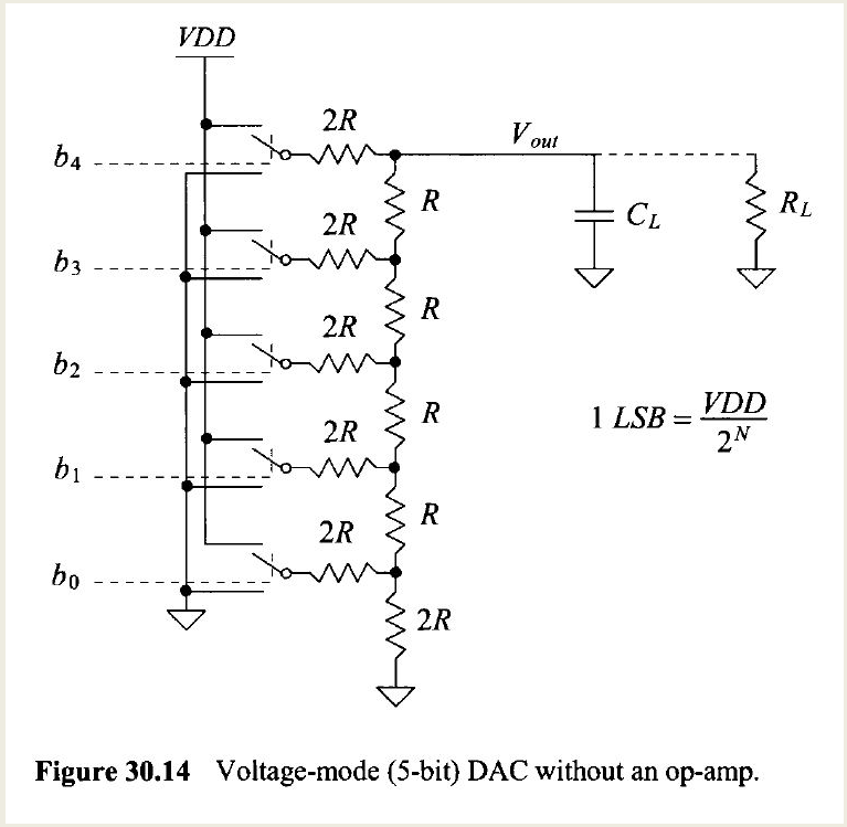
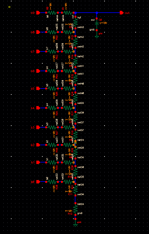
When using the R - 2R design, the output resistance can be determined by first grounding all inputs to the circuit.
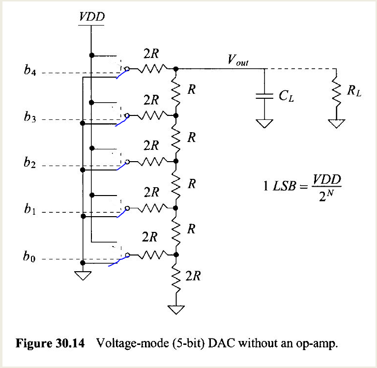
Now you can combine the resistors starting from the bottom of the circuit. 2R in parallel with 2R gives us a resistance of R.
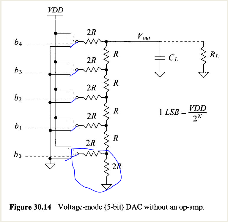
Add that in series with R, giving us 2R in parallel with 2R once again.
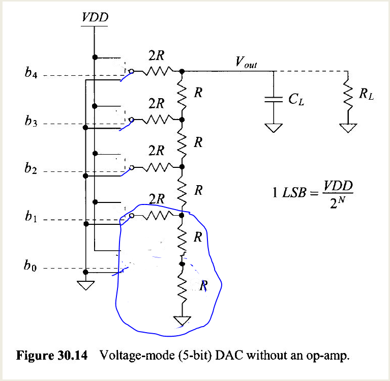
Continue this until you have one single resistance for the circuit R.
The
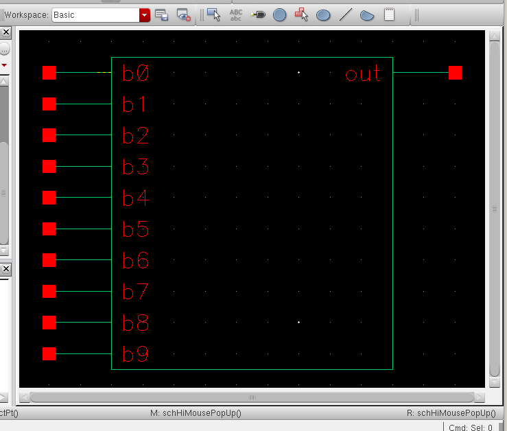
next step in the lab was to create a symbol of our schematic. in order
to do this I opened the cell view of my schematic, navigated to the
create dropdown and selected cellview from cellview. This popped up a
selection for pin names and I selected ok. The next step was to take
the symbol and create your own interpretation of that circuit by
deleting everything but the pins and creating your desired shapes. My
final product was simple but looked like this.
