
[ A2 ] symbol

[ A3 ] verification circuit

[ A4 ] simulation

[ A5 ] DRC

[ A6 ] LVS

Part B : bit cell >>>
The bit cell is accessed by NMOS pass gates that are sized not to overpower to latch.
Subsequent modules are designed to accomodate the stored data.
[ B1 ] schematic

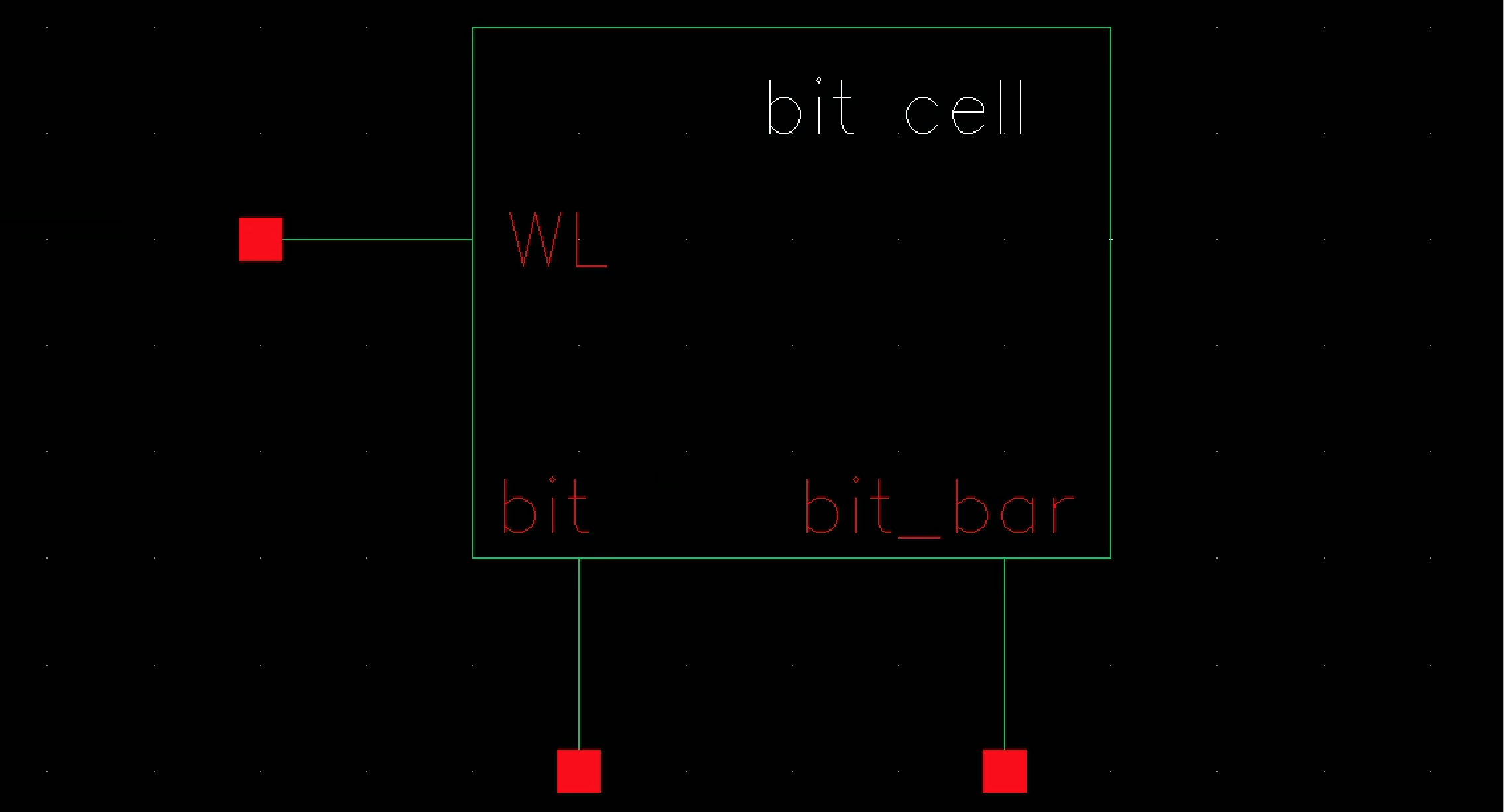
[ B2 ] symbol
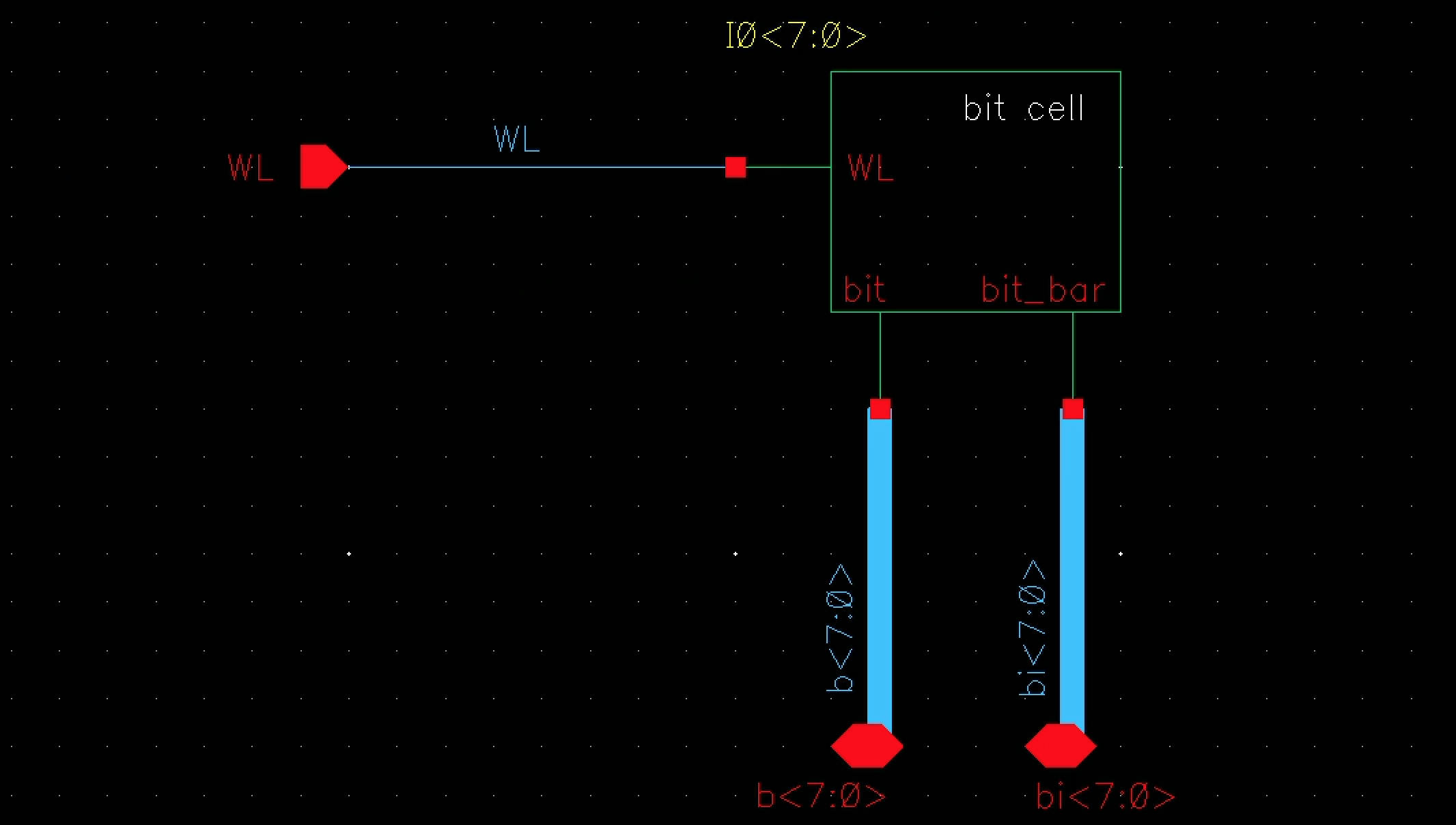
[ B3 ] verification circuit

[ B4 ] simulation, descending into the bit cell to observe the latch:

[ B5 ] DRC, the bit-cell is configured with adventageous linkage points of different metals

[ B6 ] LVS

Part C : word cell >>>
The word cell is 8 bit cells. This represents one row of the memory unit.
[ C1 ] schematic
[ C2 ] symbol

[ C3 ] verification circuit

[ C4 ] simulation, descending into bit<5>, the cells are able to receive and store data

[ C5 ] DRC

[ C6 ] LVS

Part D : word array >>>
This array is 32 word cells, completing the 32x8 design.
Included with a proper decoder, the circuit will be able to function as an SRAM.
The future work would include the pre-charger and sensitivity analyzer on this module.
[ D1 ] schematic

[ D2 ] symbol

[ D3 ] verification circuit

[ D4i ] simulation, the word line for row<0> is on a pulse source

[ D4ii ] simulation, the word line for row<10> is always on

[ D4iii ] simulation, the word line for row<20> is always off

[ D5i ] DRC, top of memory unit

[ D5ii ] DRC, bottom of memory unit

[ D5iii ] DRC success

[ D6 ] LVS

Part E: and5 >>>
Using a 5-input NAND gate and placing the inverter at the output, the AND gate is realized.
This gate will receive the row driver for further applications.
[ E1i ] schematic, preparing a NAND gate

[ E1ii ] schematic, AND gate formed

[ E2 ] symbol

[ E3 ] verification circuit

[ E4 ] simulation, the AND gate is only "1" on "11111"

[ E5 ] DRC

[ E6 ] LVS

Part F: decoder >>>
Using 31 AND gates, this decoder selects exactly 1 of 31 rows.
Larger designs may benifit from tree decoding and precoding.
The data is addressable up to 1 GHz clock speeds.
[ F1 ] schematic

[ F2 ] symbol

[ F3 ] verification circuit

[ F4 ] simulation, row<0>, row<15>, and row<31> are properley selected

[ F5i ] DRC, top of decoder

[ F5ii ] DRC, bottom of decoder

[ F5iii ] DRC

[ F6 ] LVS

Part G: SRAM >>>
The SRAM is formed by combining the word array and decoder.
This circuit is capable of storing data in each of the 256 bit cells.
[ G1 ] schematic

[ G2 ] symbol

[ G3 ] verification circuit

[ G4i ] simulation, row<16> bit<4>

[ G4ii ] simulation, row<31> bit<2>

[ G5i ] DRC, decoder joined to memory unit

[ G5ii ] DRC, inout at bottom of SRAM

[ G5iii ] DRC

[ G6 ] LVS

The circuit is ready for periphrial components.
Design files available on request.