
[ 2 ] create the NAND gate symbol

[ 3 ] build the simulation schematic

[ 4 ] simulate the NAND gate schematic

[ 5 ] layout and DRC the NAND gate

[ 6 ] extract the layout

[ 7 ] validate the layout with LVS

[ 8 ] simulate the extraction, compare to schematic


Part B : the NAND gate >>>
[ 1_NAND ] make a gate schematic using 6u/0.6u devices

[ 2_NAND ] make a symbol of the gate

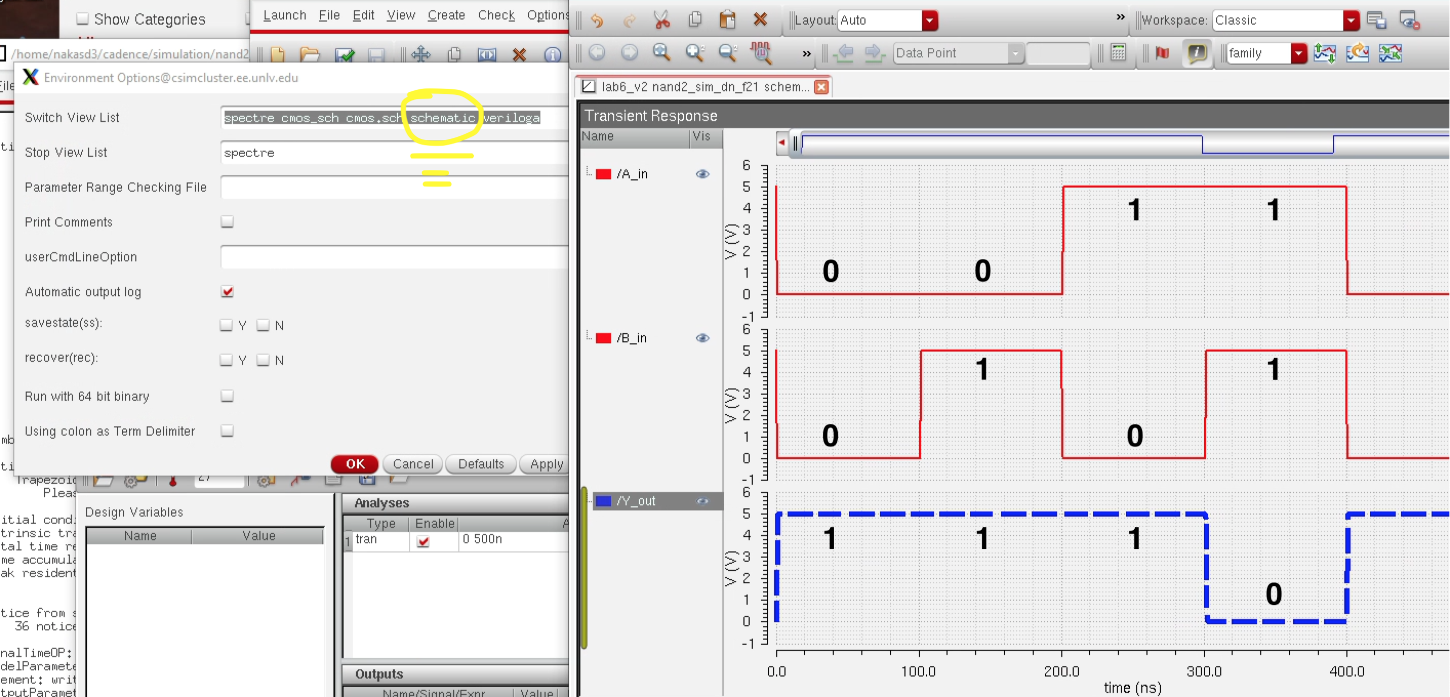
[ 3_NAND ] verify correct operation of the schematic with a testing circuit
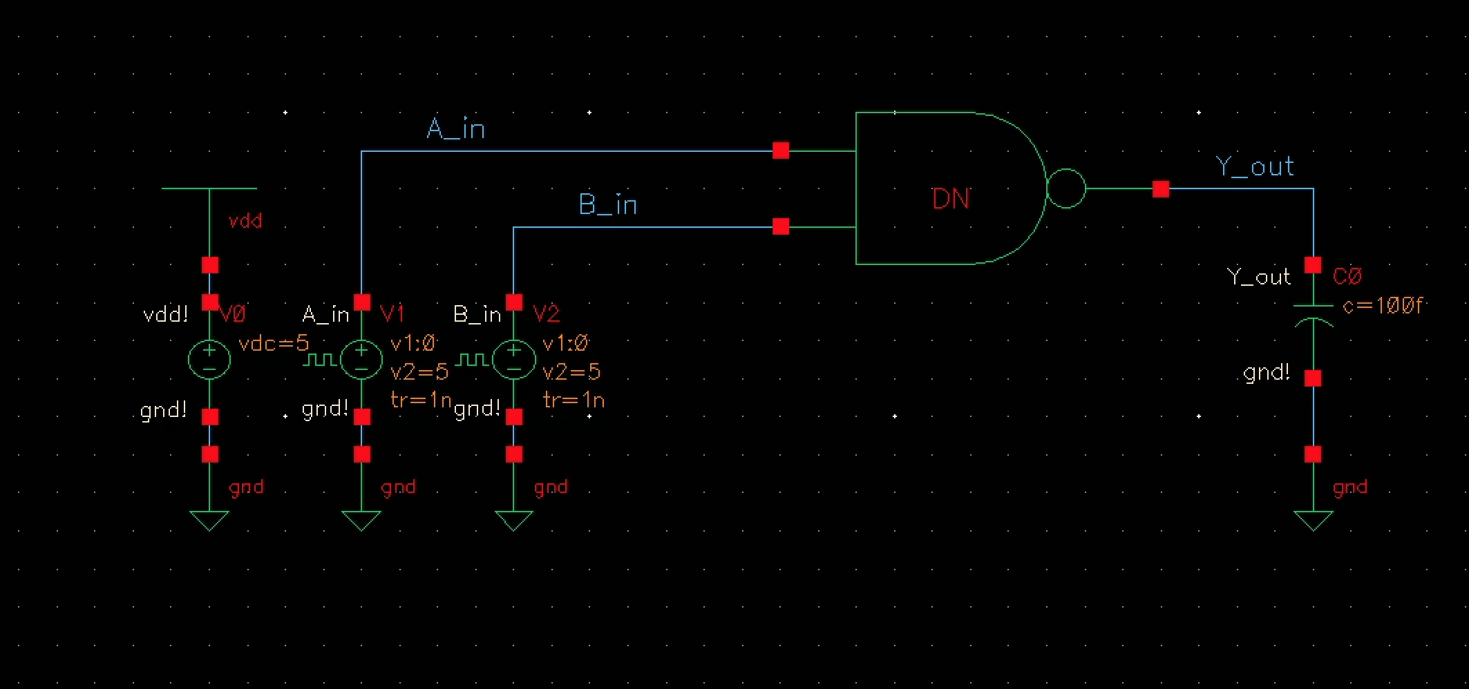
[ 4_NAND ] the results are consitent with the truth table, proceed to layout

[ 6_NAND ] extract the layout

[ 7_NAND ] verify with LVS

[ 8_NAND ] simulate the extraction, results must be same as schematic simulation

Part C : the XOR gate >>>
[ 1_XOR ] make a gate schematic using 6u/0.6u devices

[ 2_XOR ] make a symbol of the gate

[ 3_XOR ] verify correct operation of the schematic with a testing circuit

[ 4_XOR ] the results are consitent with the truth table, proceed to layout

[ 5_XOR ] layout the XOR gate and ensure DRC

[ 6_XOR ] extract the layout

[ 7_XOR ] verify with LVS

[ 8_XOR ] simulate the extraction, results must be same as schematic simulation

Part D : the full adder
[ 1_FA ] make a schematic using instances

[ 2_FA ] make a symbol of the full adder

[ 3_FA ] verify correct operation of the schematic with a testing circuit

[ 4_FA ] the results are consitent with the truth table, proceed to layout

[ 5_FA ] layout the full adder and ensure DRC


[ 6_FA ] extract the layout

[ 7_FA ] verify with LVS

[ 8_FA ] simulate the extraction, results must be same as schematic simulation

files correctly named:

design files availible on request