[ 2 ] derive the symbol

[ 3 ] design-rule-check the layout

[ 4 ] extract the layout

[ 5 ] confirm LVS

[ 6 ] build the simulation schematic

[ 7 ] adjust global values

[ 8 ] adjust step sizes

[ 9 ] simulate schematic

[ 10 ] simulate layout(extracted)

Part B : design, layout, and simulate >>>

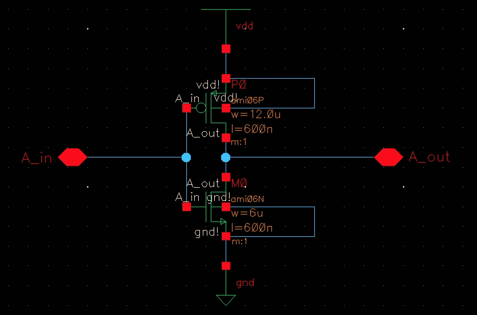
[ 1 ] draft the standard CMOS schematic

[ 2 ] create symbol of the standard CMOS schematic

[ 3 ] DRC the standard CMOS layout

[ 4 ] extract the standard CMOS

[ 5 ] LVS the standard CMOS

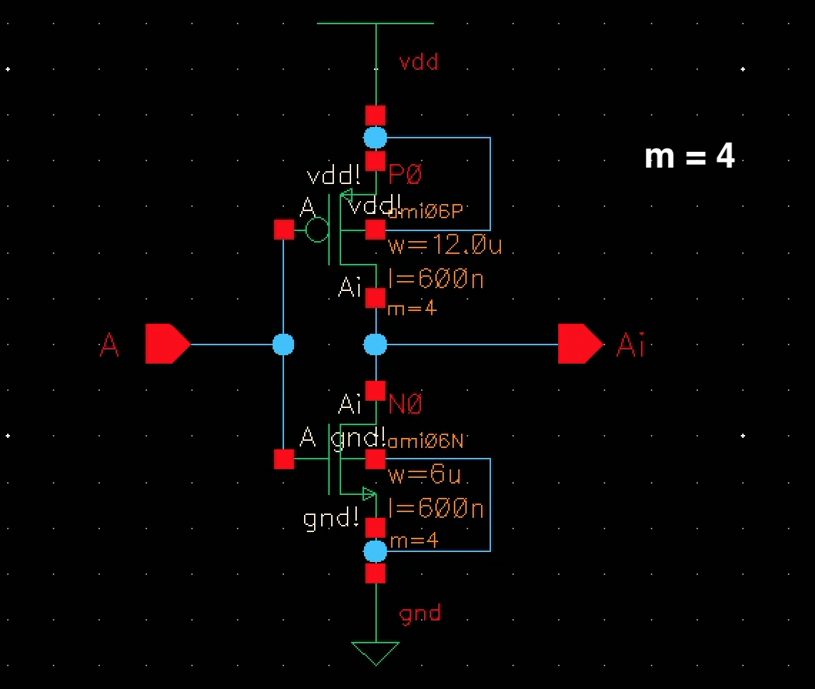
[ 6 ] draft the 4x standard CMOS schematic

[ 7 ] create symbol of the 4x standard CMOS schematic

[ 8 ] DRC the 4x standard CMOS layout

[ 9 ] extract the 4x standard CMOS

[ 10 ] LVS the 4x standard CMOS

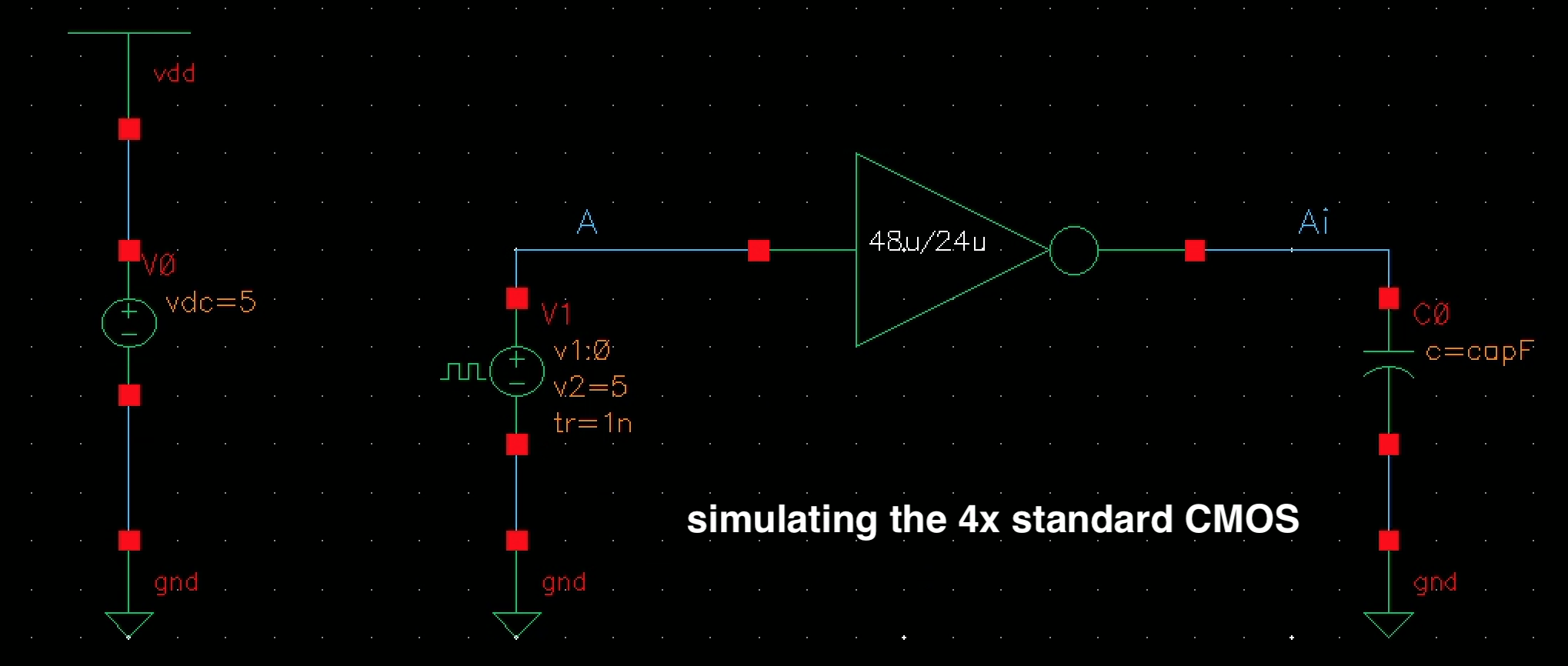
[ 13 ] prepare the standard CMOS schematic for simulation, using a variable capacitor

[ 14 ] standard CMOS schematic, 100fF, 1pF, 10pF, 100pf

[ 15 ] standard CMOS extraction, 100fF, 1pF, 10pF, 100pf

[ 16 ] standard CMOS UltraSim, 100fF, 1pF, 10pF, 100pf

[ 17 ] prepare the 4x standard CMOS schematic for simulation, using a variable capacitor

[ 18 ] 4x standard CMOS schematic, 100fF, 1pF, 10pF, 100pf

[ 19 ] 4x standard CMOS extraction, 100fF, 1pF, 10pF, 100pf

[ 20 ] 4x standard CMOS UltraSim, 100fF, 1pF, 10pF, 100pf

[ 21 ] conclusions

lab files here