
[ 2 ] make a schematic to test the symbol

[ 3 ] DRC the NMOS layout

[ 4 ] extract the layout

[ 5 ] LVS the extracted layout

[ 6 ] inspect the failure, 4 terminals implied, but only 3 exist

[ 7 ] correct the original NMOS

[ 8 ] retry the LVS

[ 9 ] simulate the NMOS schematic

[ 10 ] simulate the NMOS extracted schematic

[ 11 ] prepare the PMOS, width is double that of the NMOS

[ 12 ] complete the PMOS schematic
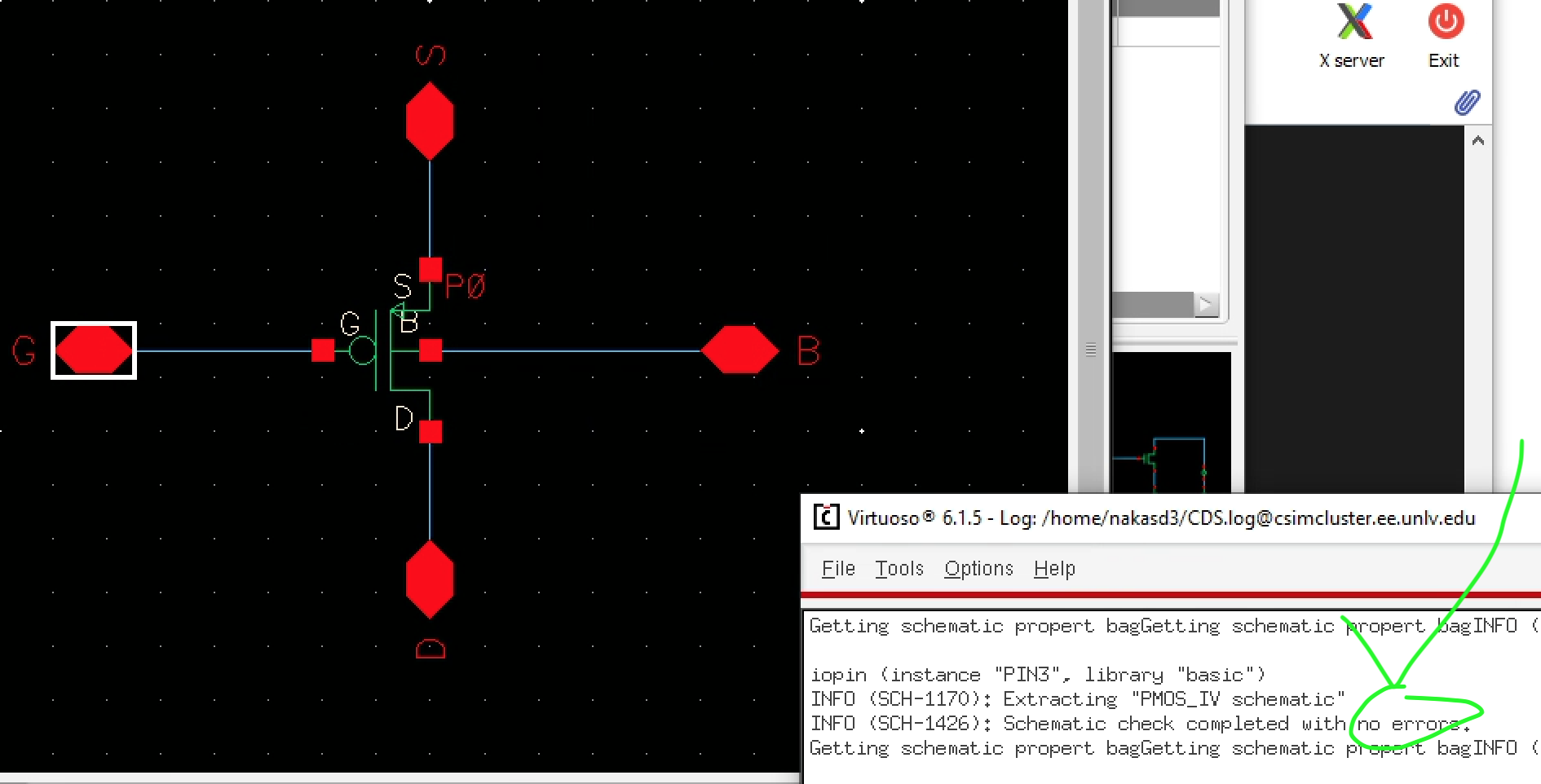
[ 13 ] create a PMOS symbol from the schematic

[ 14 ] layout the PMOS, verify with DRC
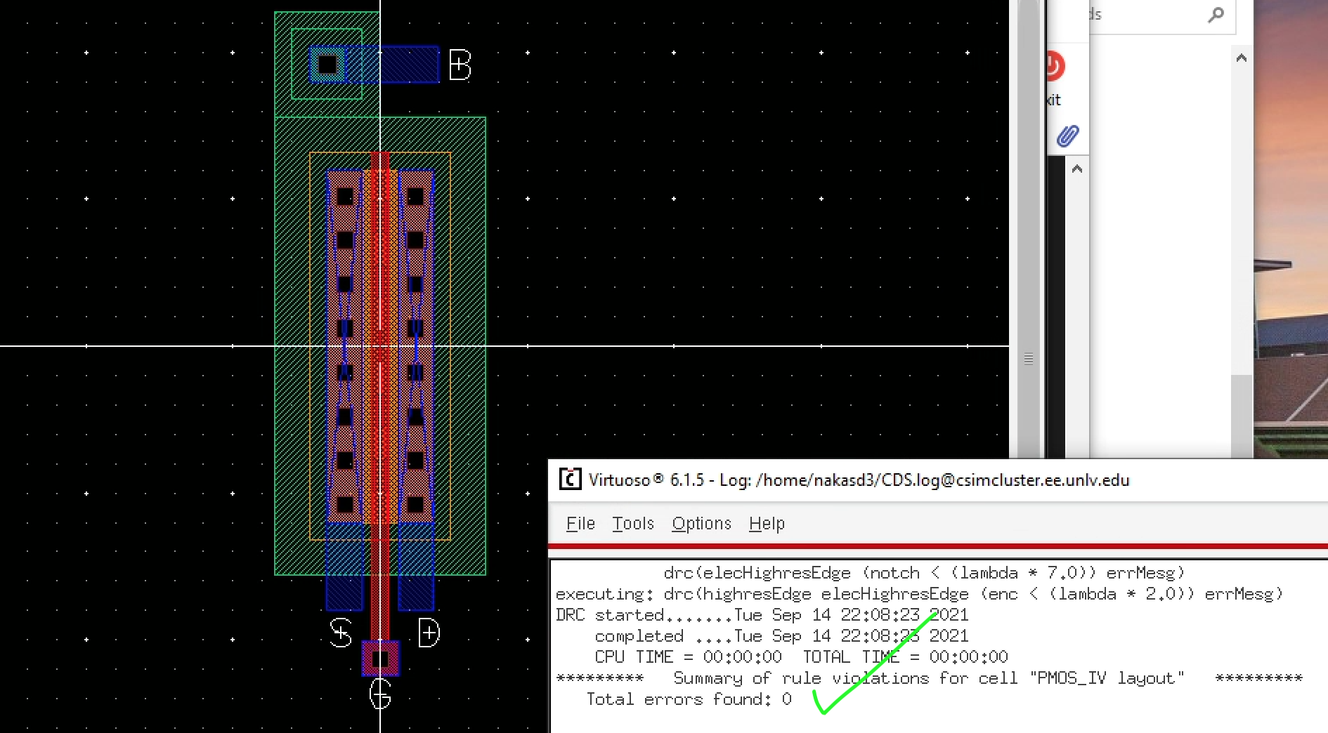
[ 15 ] extract the PMOS layout

[ 16 ] confirm the PMOS layout with LVS check

[ 17 ] ensure the simulation schematic properly supplies the PMOS
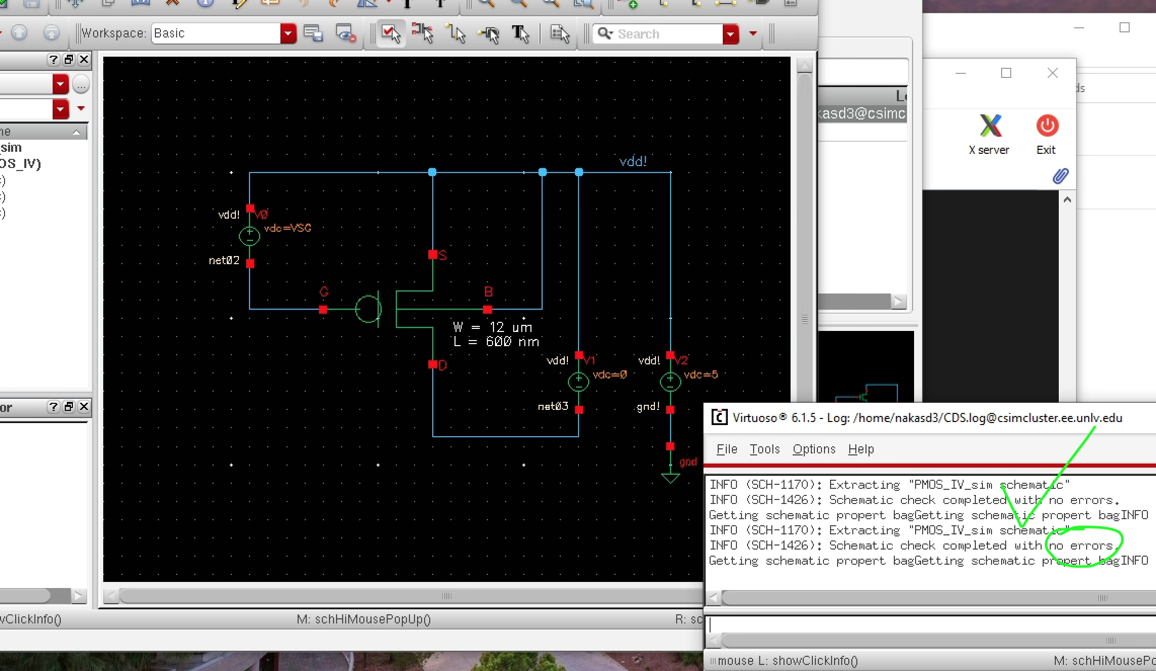
[ 18 ] simulate the PMOS schematic

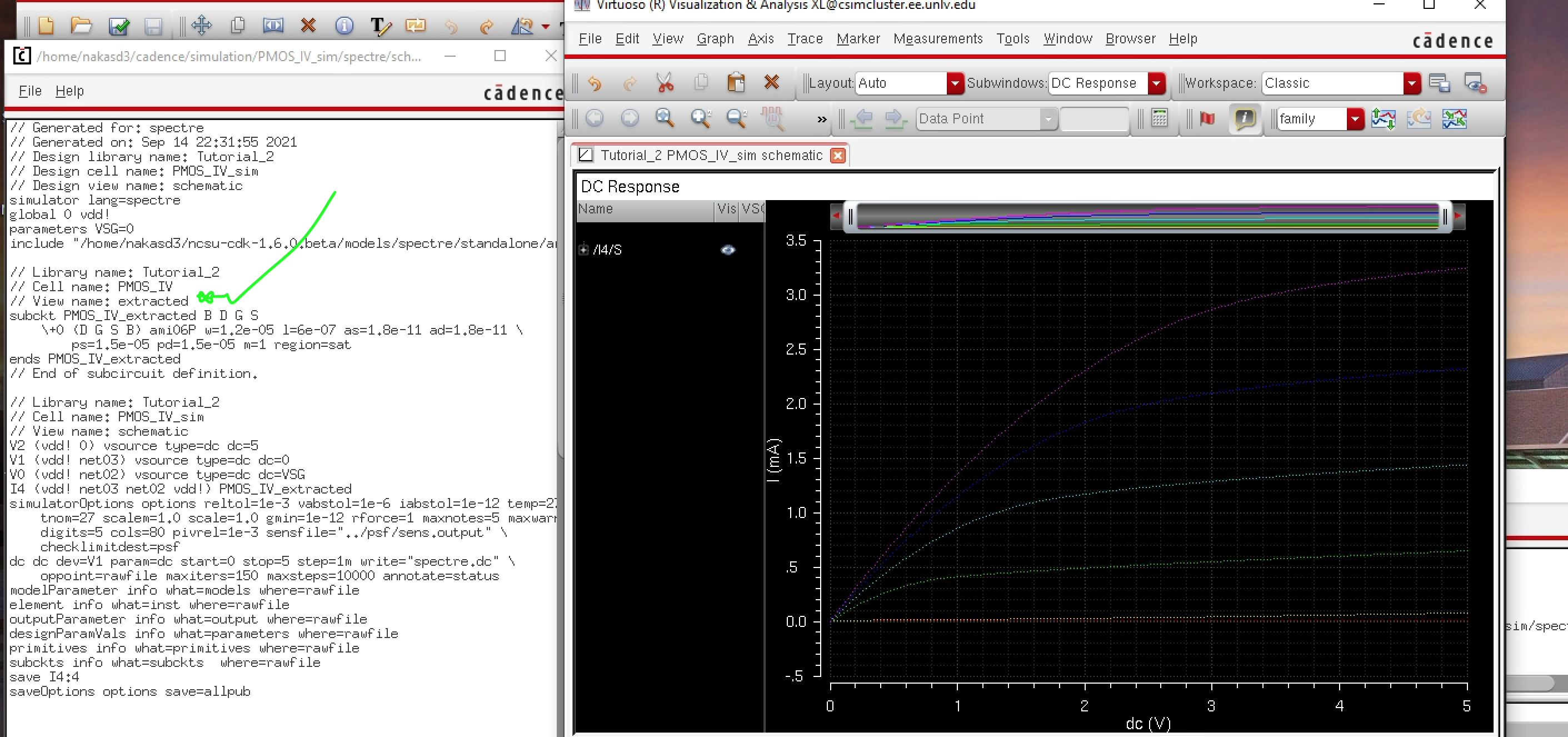
[ 19 ] simulated the extracted PMOS schematic
There are now a working NMOS and PMOS transistor. These devices can be used to make the CMOS unit. Additional verification is required during this lab.
Part B: design >>>
[ 1 ] experiment1, part 1


[ 2 ] experiment1, part 2


[ 3 ] experiment1, part 3


[ 4 ] experiment1, part 4


[ * ] before implementing the next 2 experiments, ensure the probe pad is correct:


[ 5 ] experiment2, layout 6u/.6u NMOS and connect terminals to probe pads
Create a symbol to validate the layout against:

From the schematic, the symbol is created:

Verify the symbol by simulation, exact match of previous:

Ensure layout passes DRC:

Extract and ensure LVS:

Simulate the extracted layout, design success:

[ 6 ] experiment3, layout a PMOS 12u/.6u on probe pads
Create a symbol to validate the layout against:

From the schematic, the symbol is created:

Verify the symbol by simulation, exact match of previous:

Ensure layout passes DRC:

Extract and ensure LVS:

Simulate the extracted layout, design success:

This lab built the foundation of CMOS technology.
Tutorial 2 is fundamental to applications ahead.