Matthew Daniel McDonagh NSHE:2001509804
email: mcdonm6@unlv.nevada.edu
Lab 4 – EE-421 Fall 2021
IV Characteristics and layout of NMOS and PMOS devices in ON’s C5 Process
Pre-lab: back-up all files from previous labs, begin tutorial 2 (confirm body of all NMOS devices (substrate) grounded and body of all PMOS devices (n-well) at VDD (5V) ).
Following along with Tutorial 2:
NMOS IV Schematic and Symbol:


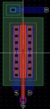
NMOS Layout and extracted view:


PMOS IV Schematic and Symbol:


PMOS Layout:

Next are the experiments, a schematic simulating I_D vs
V_DS, the NMOS is 6um x 600nm width-length, V_GS {0 :
5} V with step size 1 V and V_DS {0: 5} V with step size of 1 mV. The second
situation is V_GS {0 : 2} V with step size of 1mV and
V_DS = 100mV constant. Below is the NMOS simulation circuit and resultant graph
of a dc sweep on VGS, and a second resultant graph for VDS:


Next part is the schematic simulating I_D vs V_SD on the
PMOS, 12um x 600nm width-length, with V_SG {0 : 5} V with step size of 1V and
V_SD {0 : 5} V with step size of 1 mV, and a second simulation of I_D vs V_SG
where V_SG {0 : 2} V with step size of 1 mV and V_SD = 100mV const. Below is
the PMOS Simulation circuit and resultant graph of a dc sweep on VDS, and a
second resultant graph for VGS:


Both of the simulations for the VDS going from 0 to 5 and the simulations for the 1mV steps from 0 to 2 volts for both PMOS/NMOS required by the lab were done above as part of the prelab. Prior to the next part, we must confirm that the probe pad is constructed correctly, as well as any possible connection modules:


Next is a schematic and layout of the NMOS with 4 of the probe pods attached:


Next is making sure LVS passes matching and DRC check confirms:


Next is a schematic and layout of the PMOS with the 4 probe pads attached:


Next is a confirmation that the LVS passes matching and the DRC check confirms:


Conclusion, files are backed up on my google drive, and this lab was very helpful with learning the fundamentals of CMOS technology.