Lab Project - EE 421L
Authored
by Charlene Drake
Email: drakec2@unlv.nevada.edu
November 24, 2021
Lab Description
For
this project we will be designing a Register File that 32 8-bit words.
In order to access these words, we will use 5-bit address. Other inputs
of the RF include the 8-IO lines for reading and writing, a control
signal, RW which indicates a read or write to the RF, and VDD/gnd.
Project Components
- SRAM Cell
- 8-bit SRAM
- 32-bit Array
- 5 input AND Gate
- Row Decoder
- Register File
SRAM Cell
The
first component needed for the design of our RF was the SRAM which
stores data as well as determines where data is read and written from.
The SRAM is composed of a two NMOS devices and two 1.5u/1.5u inverters.
The inverters have a very small width in order for easy flipping of the
cell. For the inputs we have D, Di, and RL. When RL is high, data is written and when RL is low data is no longer written.
Schematic:

Symbol:

Layout:

DRC:

Extracted:

LVS:

Simulation:


As you can see, whenever the RL is high, the value for D is stored and
output, and when the RL is low, that previous value for D is kept continues to be output.
8-bit SRAM
Next we needed to design an 8-bit SRAM which consisted of 8 of the SRAMs
that we had previously designed. We were able to accomplish this design
with arrays. By going into the SRAM's properties we are able to declare
an array which duplicated the instance 8 times. We then needed to run 8
lines of data into D and Di which is also done with arrays and busses.
Schematic:

Symbol:

Layout:

The layout for the 8-bit SRAM is pretty much the same as the SRAM, we
just needed to instantiate the design 8 times total and then connect
all of the RL's.
DRC:

Extracted:

LVS:

Simulation:


As
you can see, the simulation for the 8-bit SRAM is the same as the 1-bit
SRAM. When RL is high I0<0> follows D<0> and I0<1>
follows D<1> but as RL goes low the last value from D<0>
and D<1> is kept and output for I0<0> and I0<1>.
32-bit Array
Next, we create the 32-bit array which stores the memory for the 32, 8
bit words. We do so by instantiating the 8-bit SRAM we had previously
designed, 32 times. Once again, this is done with an array. Since there
are 32 8-bit SRAM we also need 32 RL's which we create with a bus.
Schematic:

Symbol:

Layout:


DRC:

Extracted:

LVS:

5 input AND Gate
Now we can design the 5 input AND gate that will be used with the row
decoder to assign addresses to each of the 32 8-bit words. We do so
with 6 NMOS devices and 6 PMOS devices.
Schematic:

Symbol:

Layout:

DRC:

Extracted:

LVS:

Simulation:


As you can see, the AND gate is functioning properly and only outputs a 1 when all inputs are 1.
Row Decoder
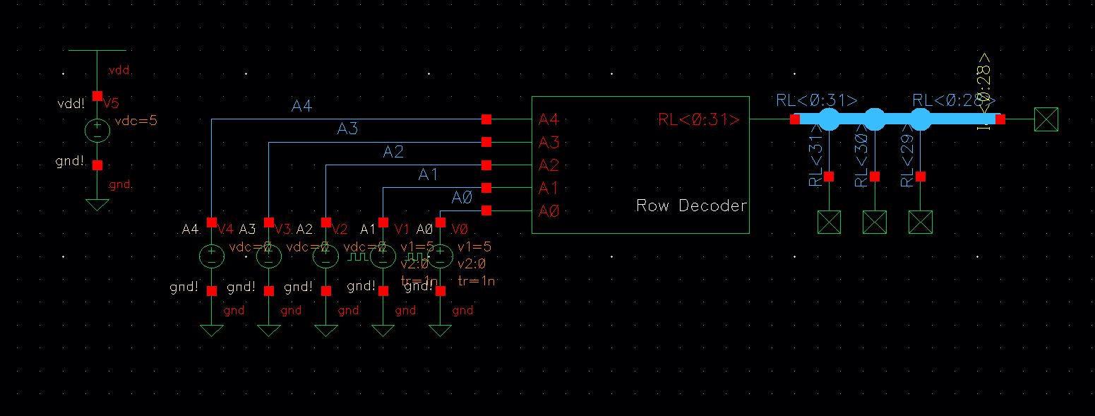
Next we design the row decoder which assigns a 5-bit address to each 32
8-bit word. As you can see, labeling the busses was quite intense as we
needed to ensure 00000-11111 was passed through the AND gate as those
are the addresses that the 32 8-bit words were assigned to.
Schematic:

Symbol:

Layout:


DRC:

Extracted:

LVS:

Simulation:


As you can see, the row
decoder is functioning properly. At address "00000" RL<31> is on,
whereas at address "00001" RL<30> is on, and at address "00010"
RL<29> is on.
Register File
Now that all of our componenents have been designed, we are able to
design our Register File. To do so we take our row decode, and connect
the RL to the RL of our 32-bit Array. We also have our 5 inputs for the
address feeding into the row decoder and then the buses for D and Di
feeding data into the 32-bit array.
Schematic:

Symbol:

Layout:


For the layout of the RF we instantiate the layouts of the row
decoder and the 32-bit array, and connect them at their RL's.
DRC:

Extracted:

LVS:

Simulation:


As you can see the register file is functioning properly. When
Ain is high we are calling the address "00001" which writes to
RL<30>. This makes I0<30> follow D<0>. When Ain is
low, the address "00000" is being called to and we are writing to
RL<31> so now I0<31> follows D<0>.
Design Files
Return to Lab Directory