

Lab 4 - EE 421L
2) Generate
a schematic for simulating ID v. VGS of an NMOS device for VDS = 100 mV
where VGS varies from 0 to 2 V in 1 mV steps. Again use a 6u/600n
width-to-length ratio.


3) Generate a schematic
for simulating ID v. VSD (note VSD not VDS) of a PMOS device for VSG
(not VGS) varying from 0 to 5 V in 1 V steps while VSD varies from 0 to 5 V in 1 mV steps. Use a 12u/600n width-to-length ratio.


4) Generated a schematic for simulating ID v. VSG of a PMOS device for VSD = 100 mV where VSG varies from 0 to 2 V in 1 mV steps. Again, use a 12u/600n width-to-length ratio.


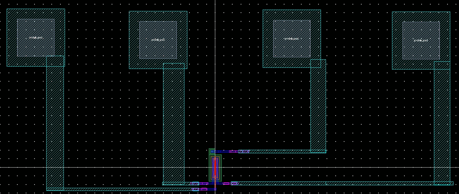
6u/0.6u NMOS Layout with Bonding Pads
For the next part of the lab, I layed out a 6u/0.6u NMOS and connected all 4 MOSFET terminals to probe pads.
Below is the schematic that the layout is based off of.

Here is the symbol that was created for the NMOS.

Finally, here is the layout of the NMOS.


Below is the extracted version.


I ensured that the NMOS was LVS and DRC clean.


12u/0.6u PMOS Layout with Bonding Pads
For the last part of the lab, I layed out a 12u/0.6u PMOS and connected all 4 MOSFET terminals to probe pads.
Below is the schematic that the layout is based off of.

Here is the symbol that was created for the PMOS.

Finally, here is the layout of the PMOS.

Below is the extracted version.


I ensured that the PMOS was LVS and DRC clean.

