Lab Project - EE 421L
Damian Aceves Franco
acevesfr@unlv.nevada.edu
11/24/2021
Project (NOT a group effort) – design a register file (RF) that uses an 8-bit word and has 32 words. The RF uses a 5-bit
address to access the 32 8-bit words. Other inputs to the RF are the 8-IO lines for reading and writing, a control signal, RW,
for indicating either a read or write to the RF, and VDD/ground.
First half of the project (schematics and design discussions) of your design and an html report detailing
operation (including simulations), is due at the beginning of lab on Nov. 17.
Put your report (proj.htm) in a folder called /proj in your directory at CMOSedu and link to your index.htm page.
Dr. Baker will go over your design with you (in person), including running simulations, when lab meets on Nov. 17.
Your report should show reading and writing to the RF at various addresses.
Second half of the project, a verified layout and documention (in html), is due at the beginning of lab on Nov. 24.
Dr.
Baker will meet with you on Nov. 24 to go over your layout and,
again, put your report in the /proj folder in your directory at
CMOSedu.
Ensure that there is a link on your project report webpage to your zipped design directory.
*************************************
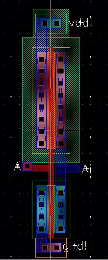
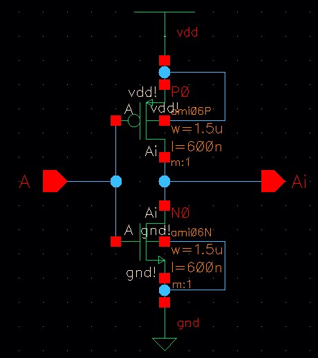
Inverter 12u by 6u
create an inverter
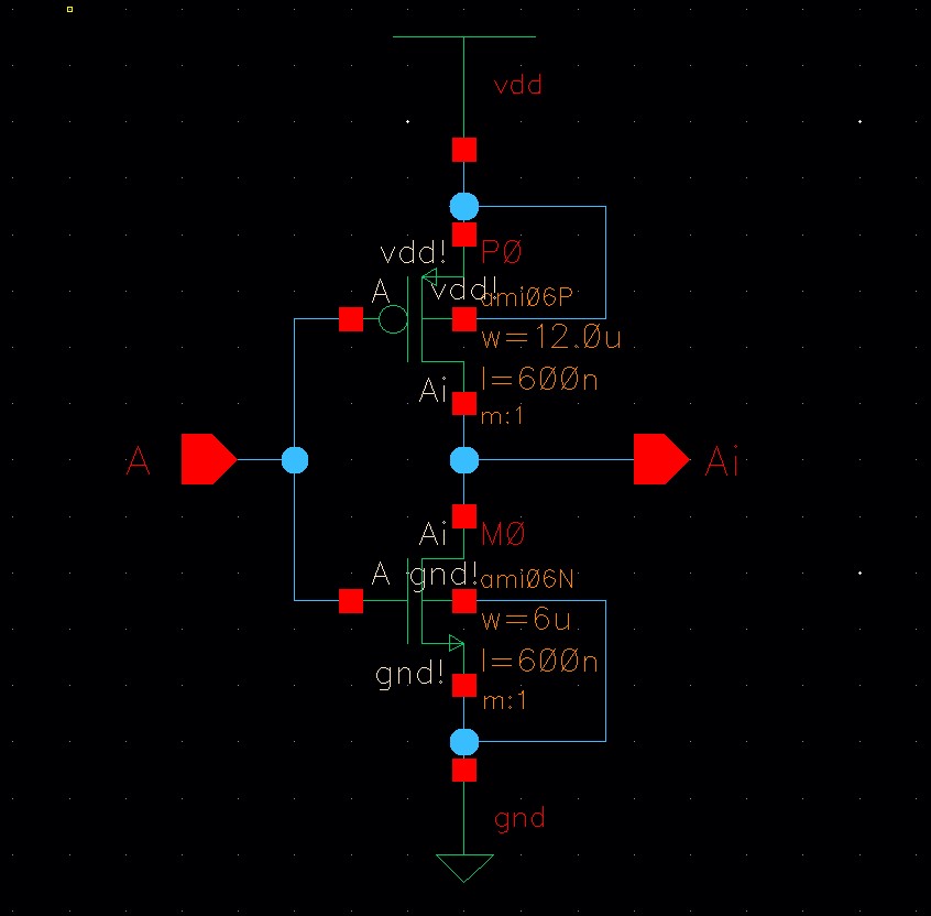
symbol

layout of the inverter will be needed later
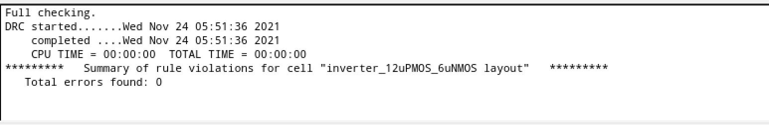
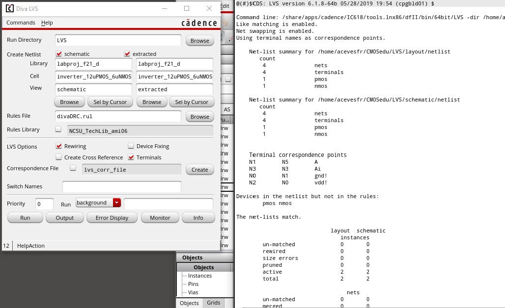
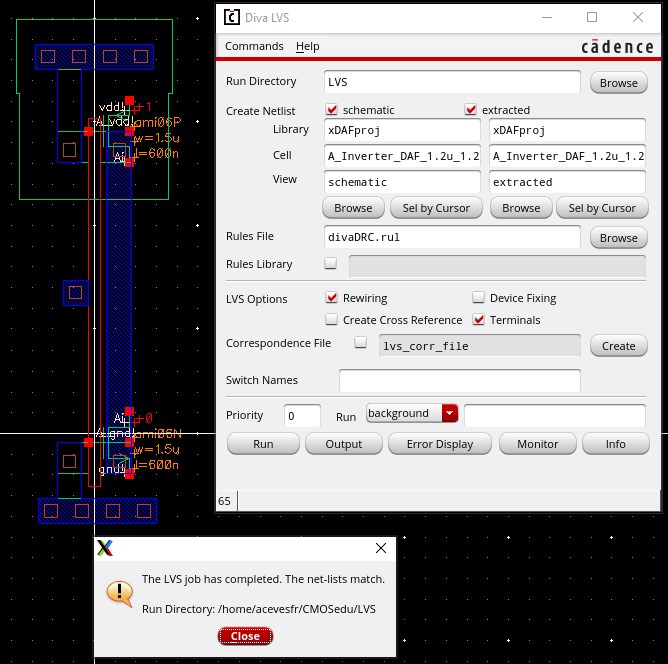
DRC and LVS
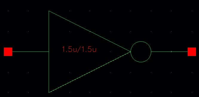
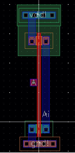
Inverter 1.5u by 1.5u
SRAM Schematic
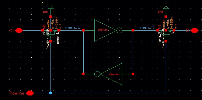
firsrt part of the project design is making the Static Random Access Memory (SRAM). This cell contains 1-bit of data.
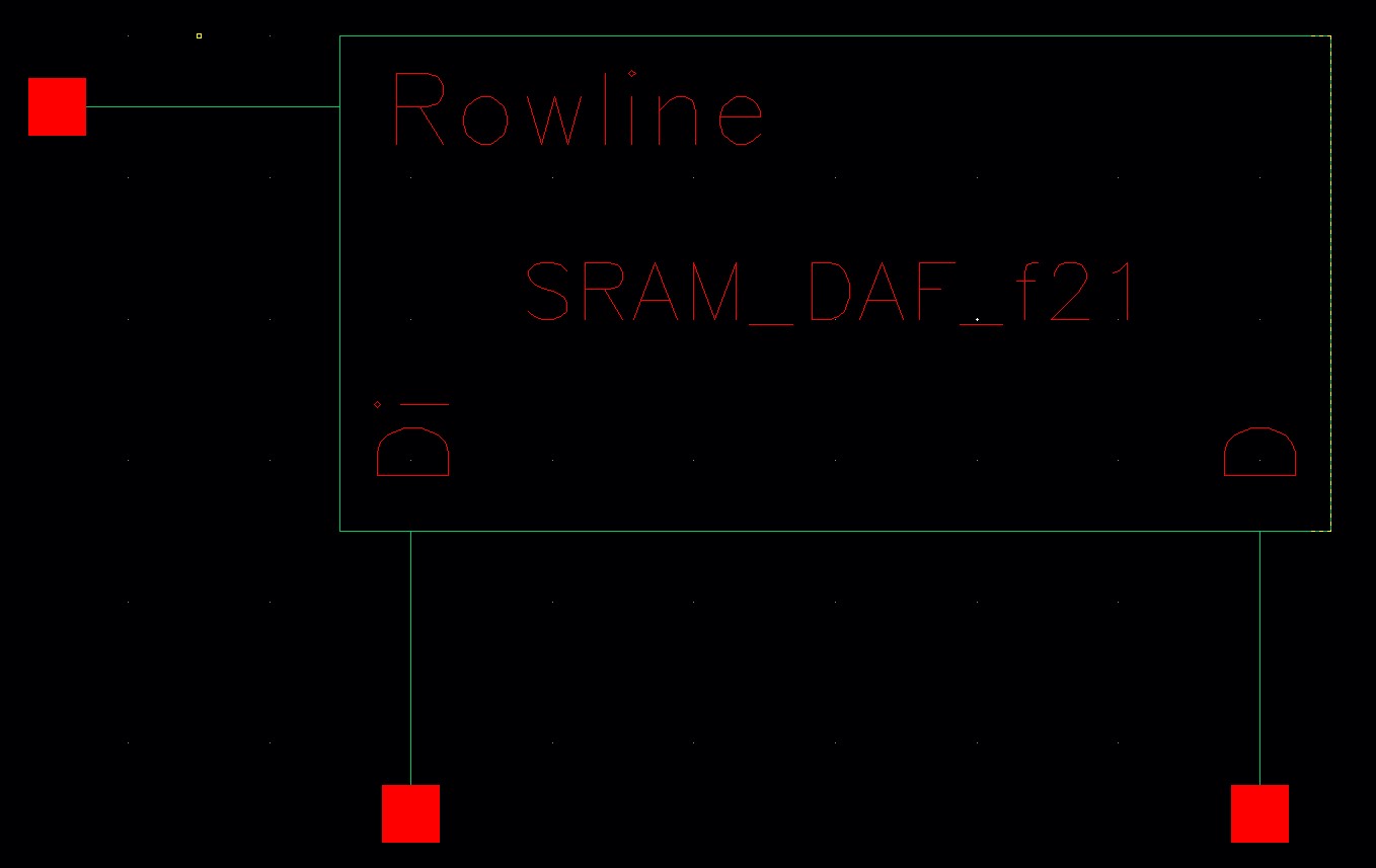
SRAM Symbol
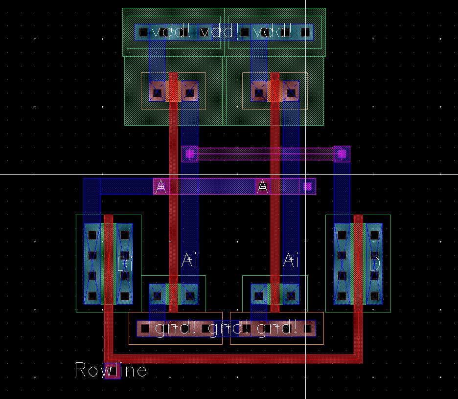
layout
Below is the layout of the memory cell. It consists of two inverters and two NMOS devices.
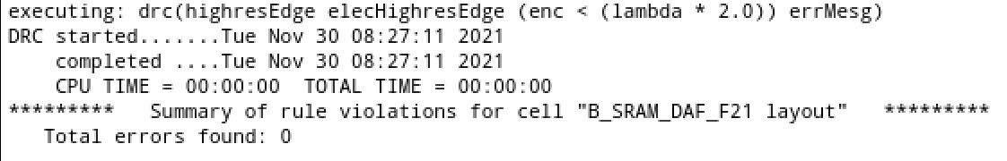
DRC
extract and LVS
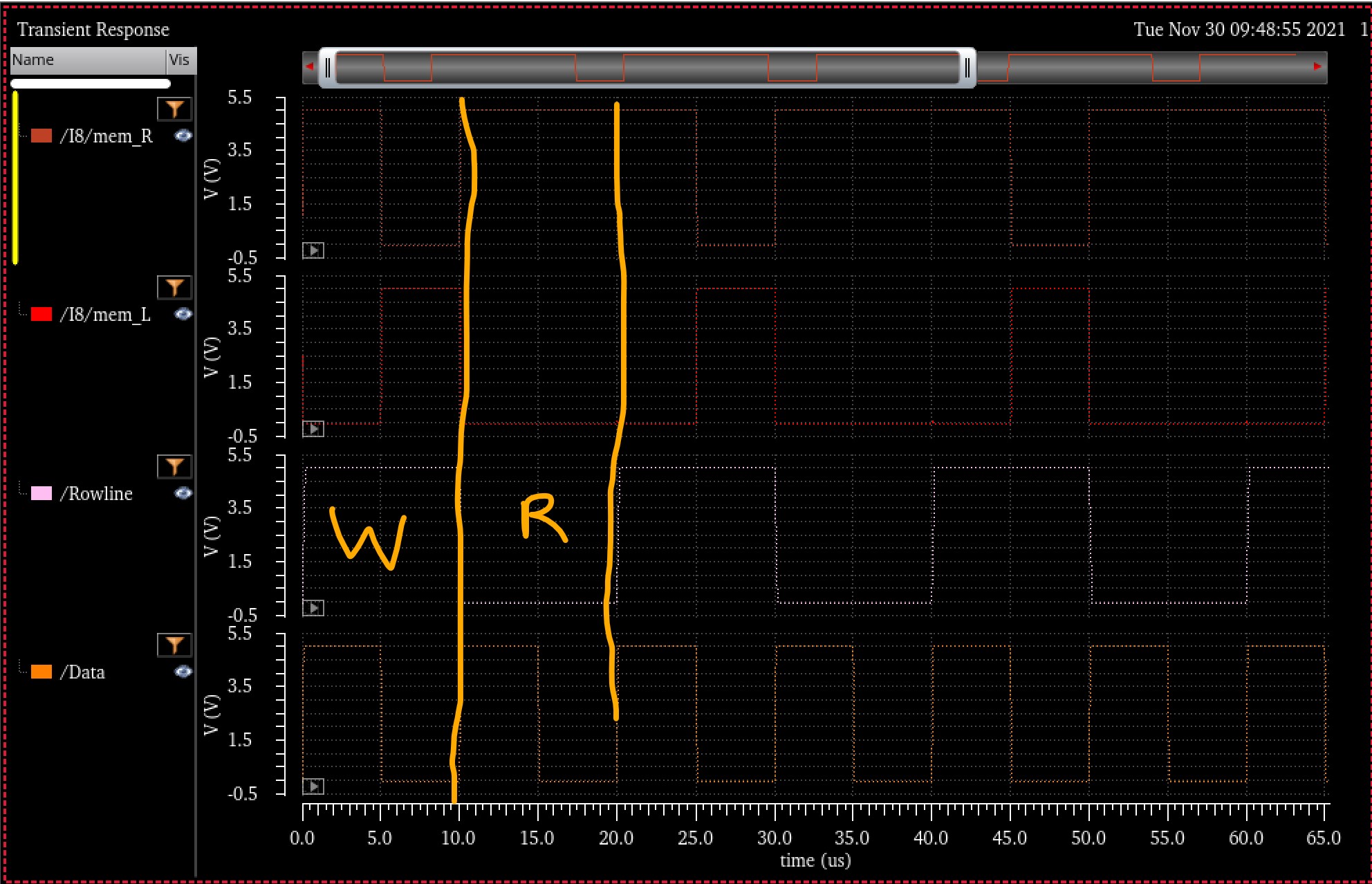
sim
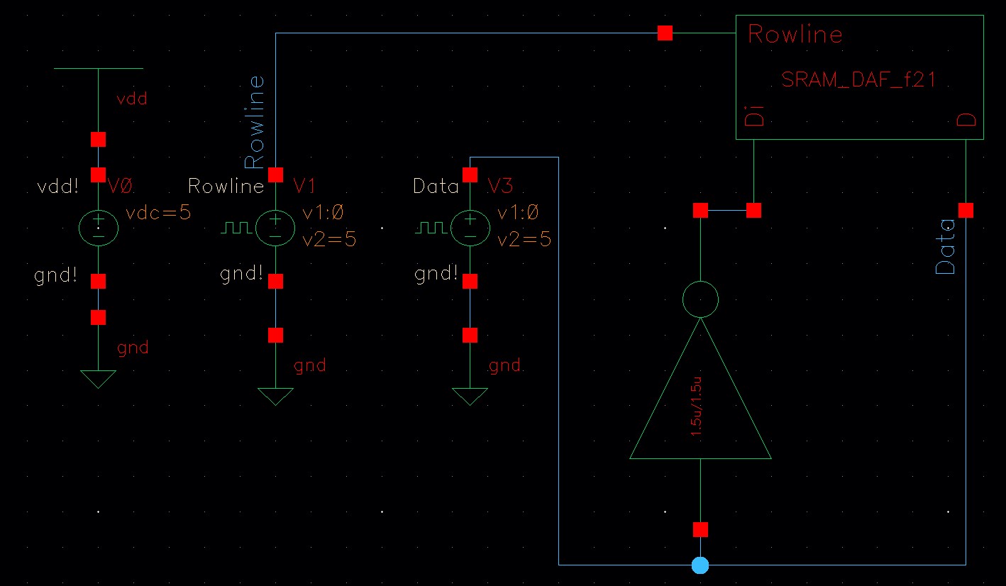
The results of the test simulation are as expected
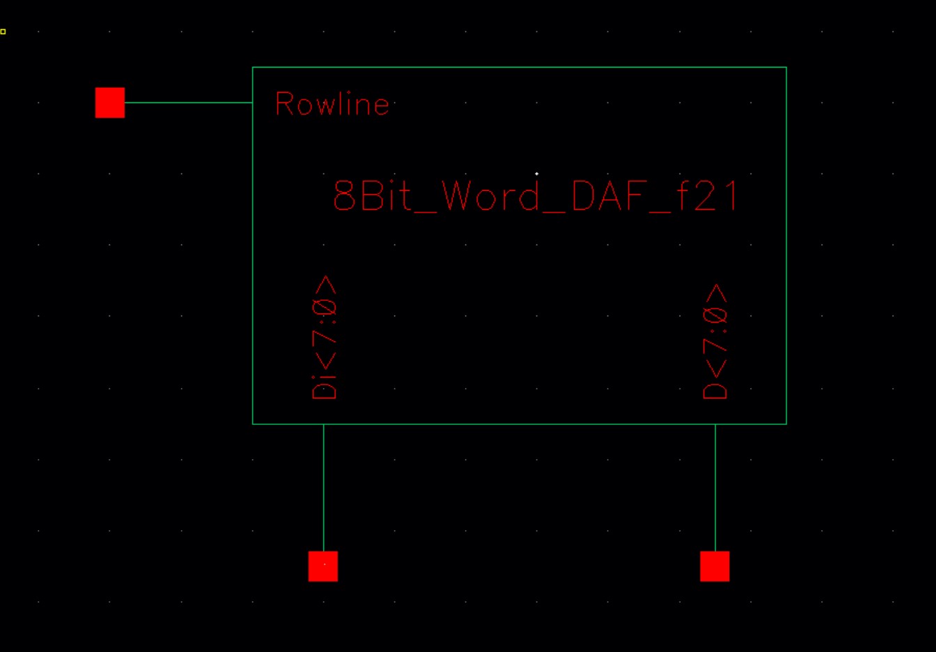
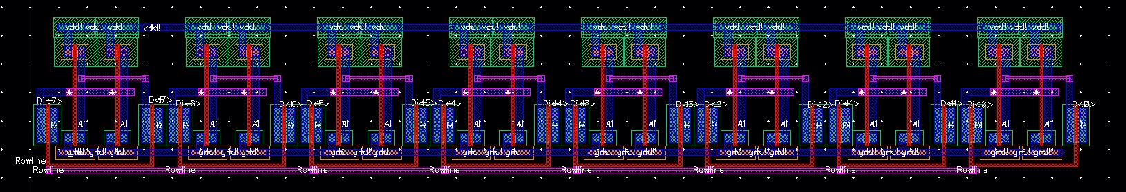
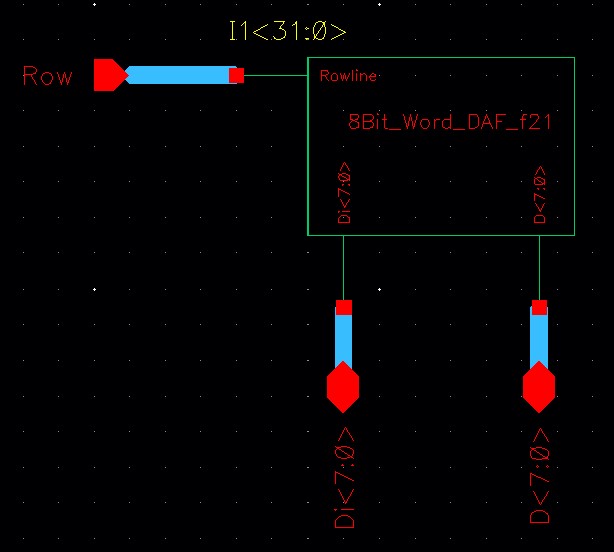
8-Bit Word Schematic and symbol
Our word is made from 8 SRAM cells in other words an array of 8-bit memory cells
The row input is kept as a single node
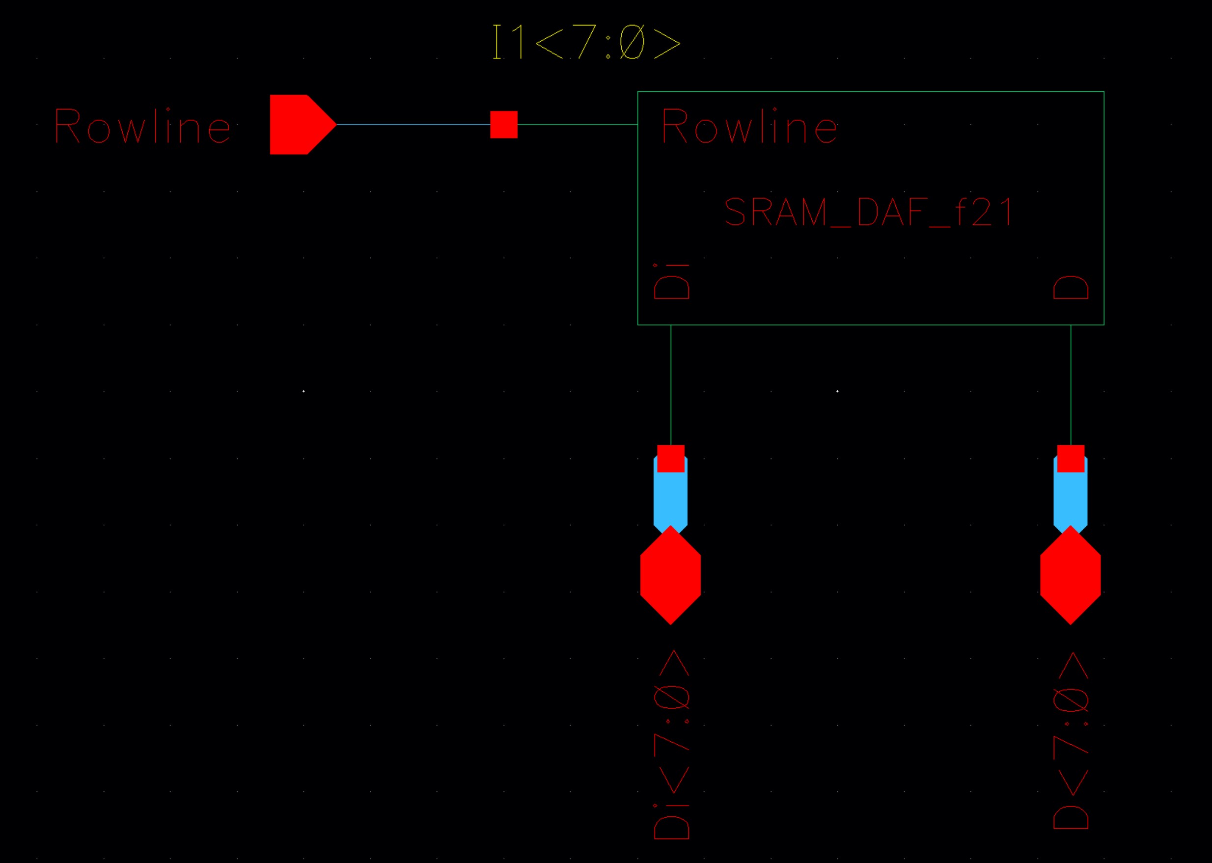
Symbol
Layout
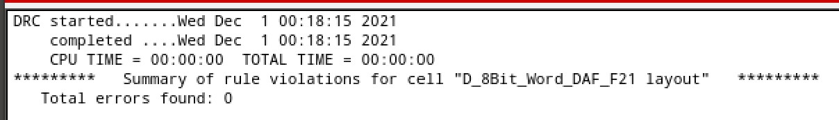
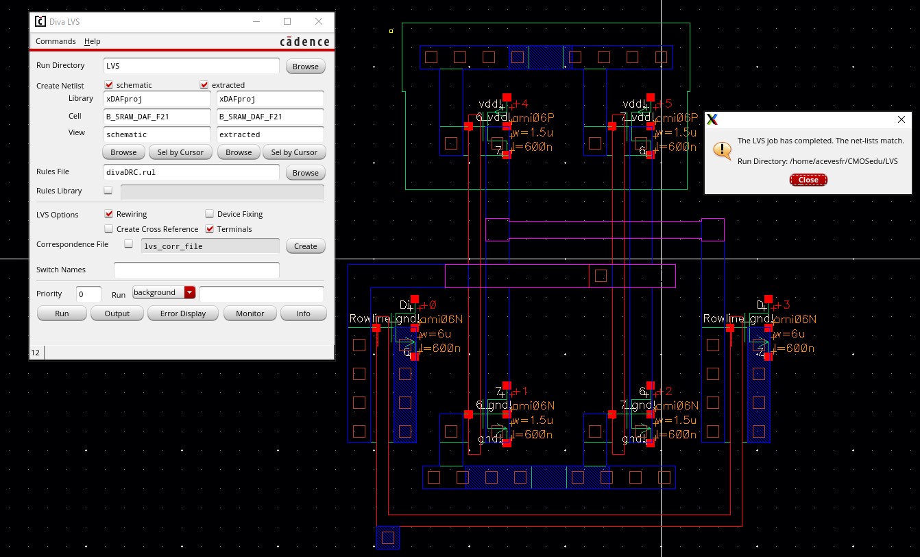
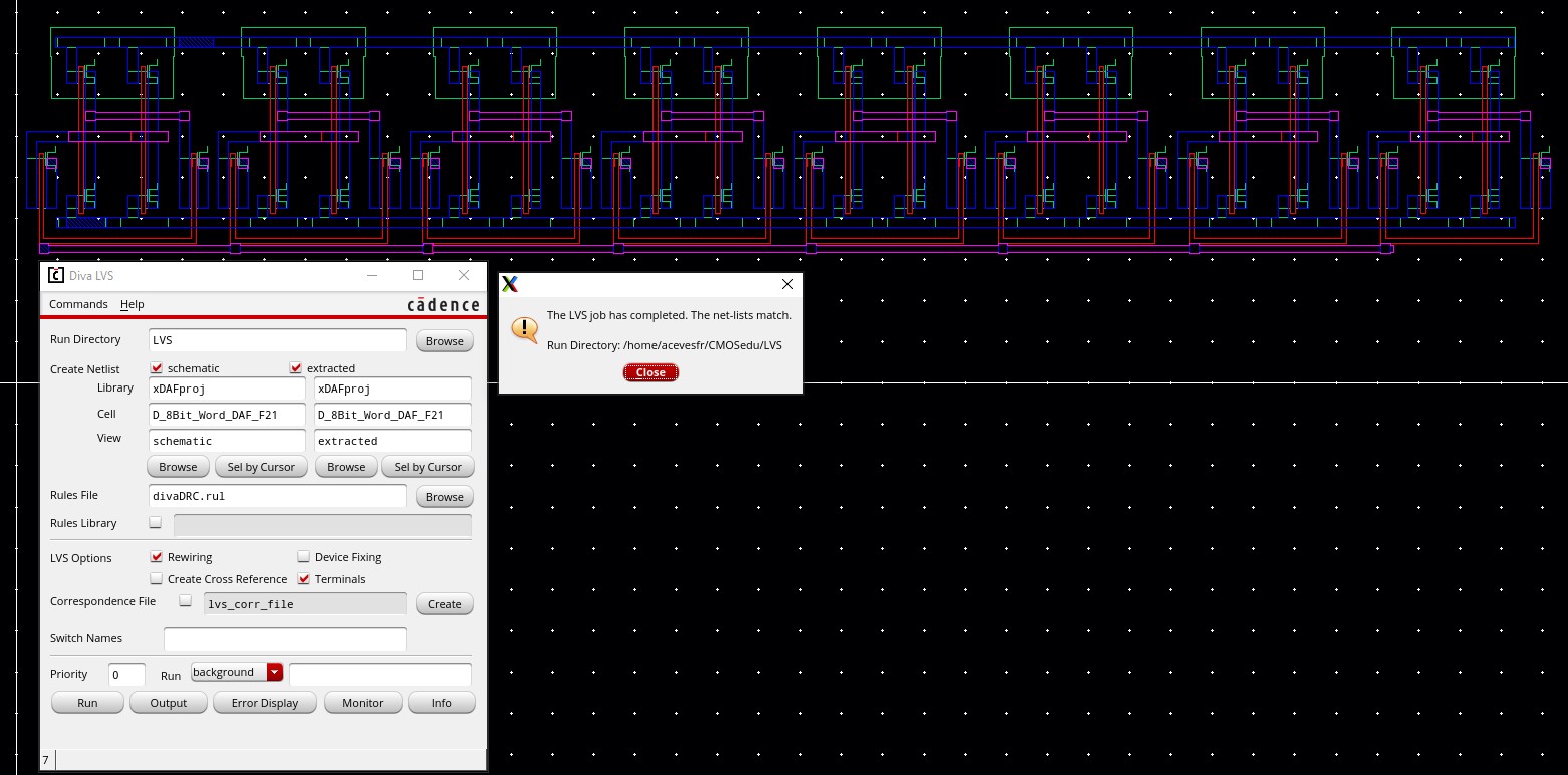
Extract and LVS
Sim
The results of the test simulation are as expected
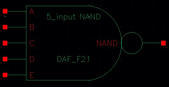
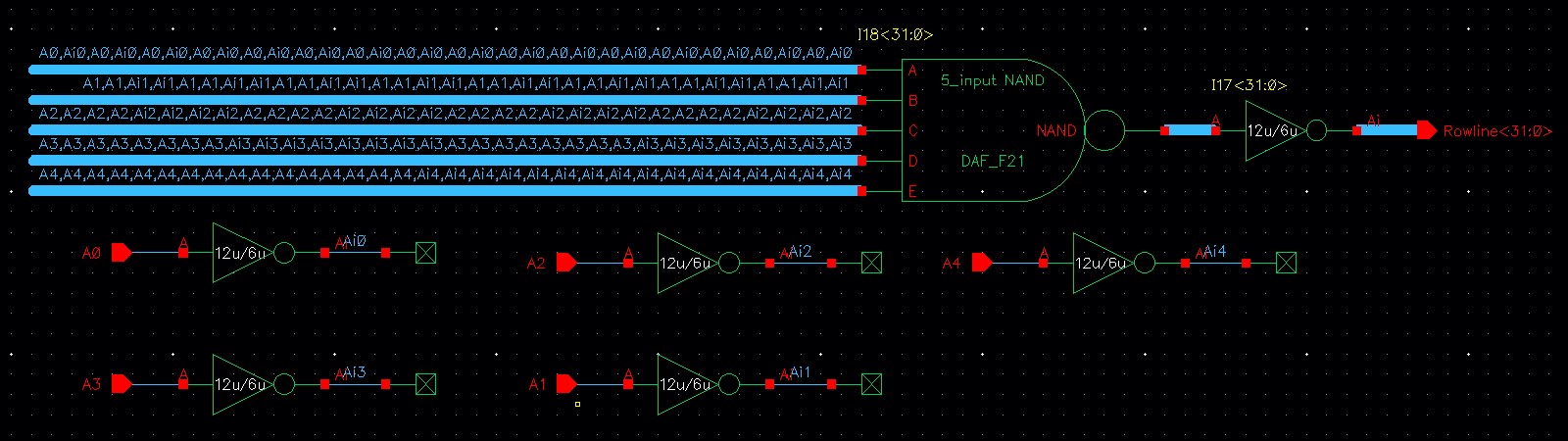
5-input NAND Gate and Symbol
The NAND Gate will be used to implent the Row Codecoder having 5-inputs and one output
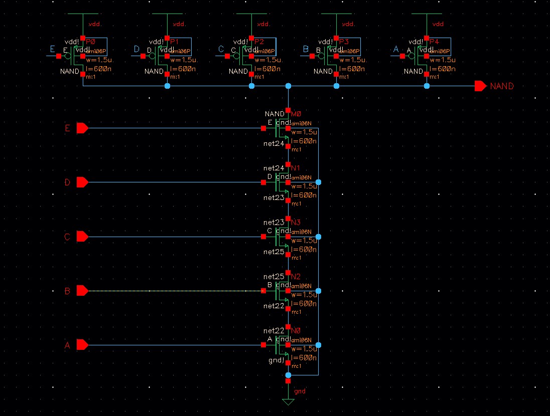
Symbol
Layout
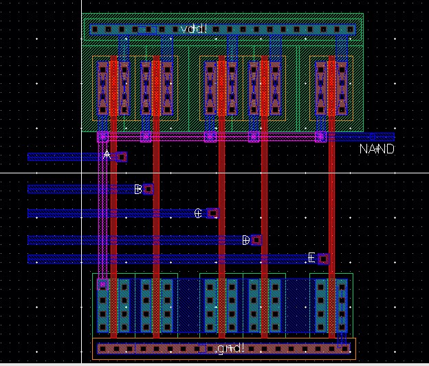
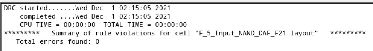
DRC
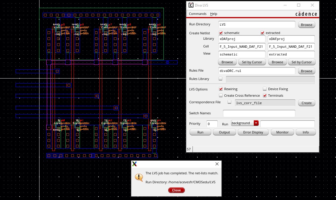
Extract and LVS
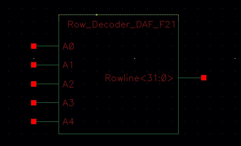
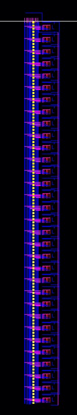
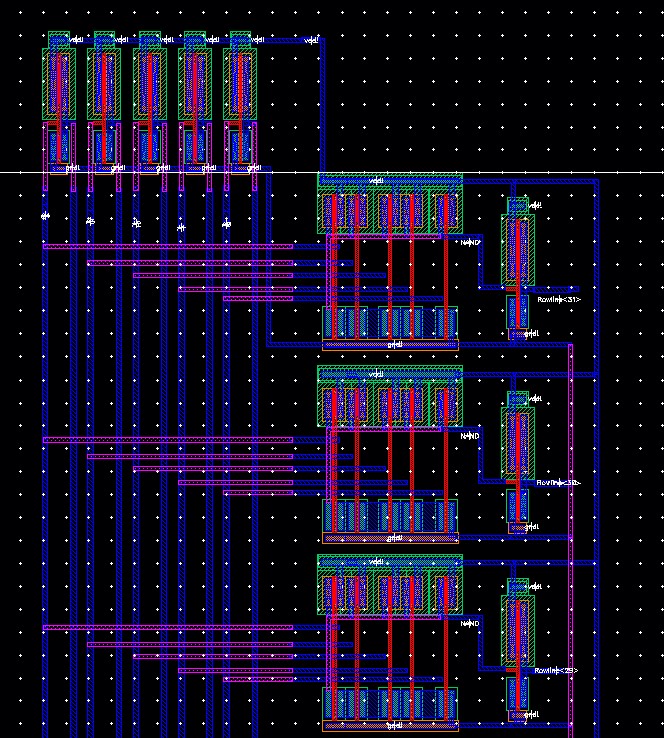
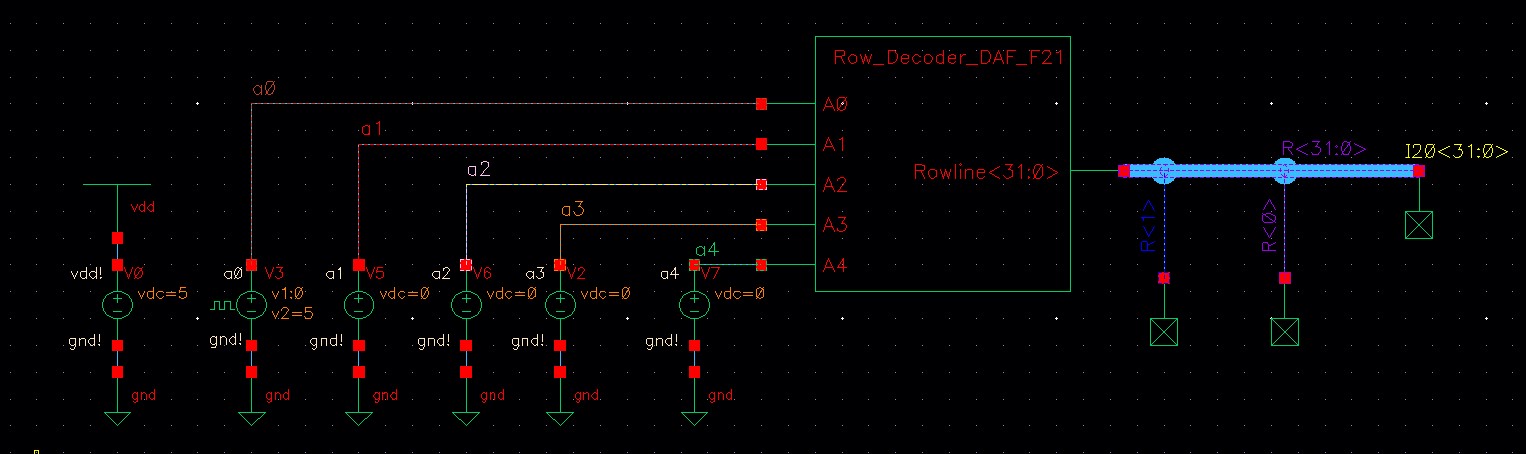
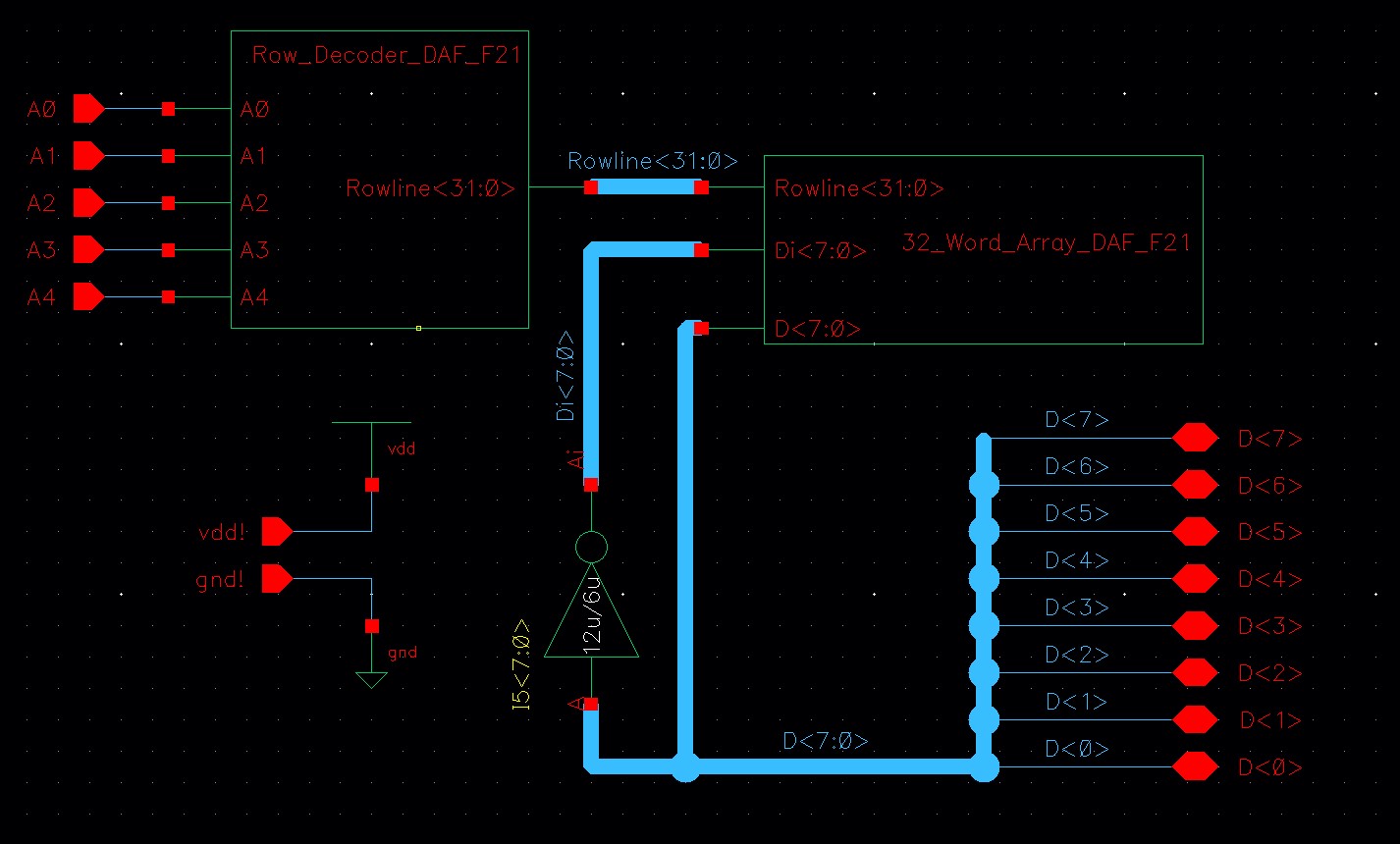
Row Decoder
row decoder lets us know what 8-bit cell is being accessed
In order to keep a clean schematic, busses and arrays were used
Symbol
Layout
32 NAND instances and has five of the outputs pulled that matches its assigned address,The first instance has an addres of "11111" then "11110........to "00000"
DRC
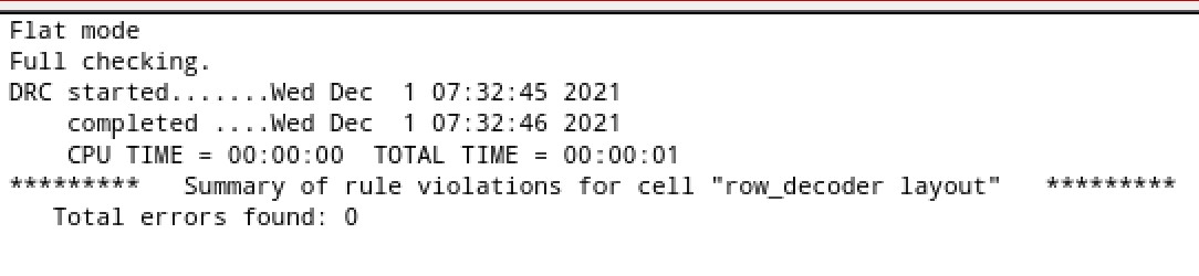
Extract and LVS
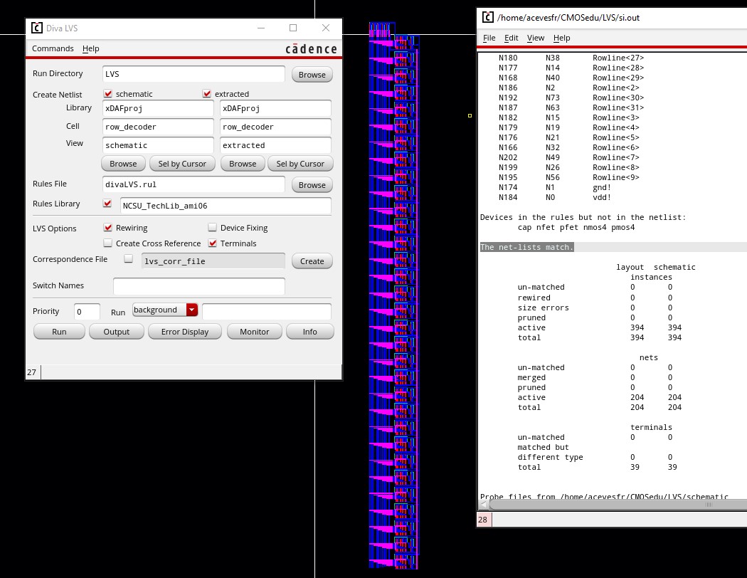
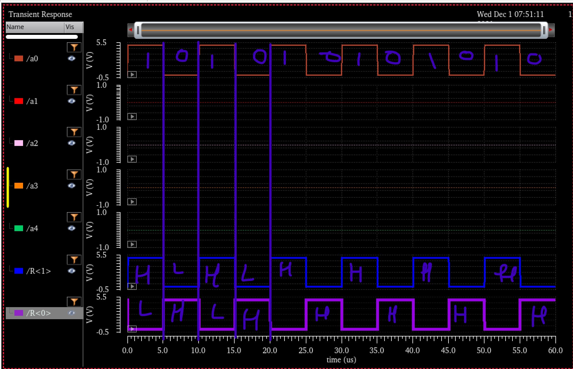
SIM
Simulation results are right
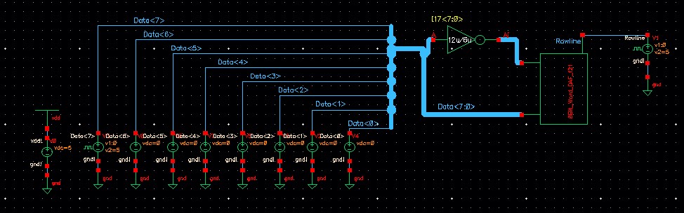
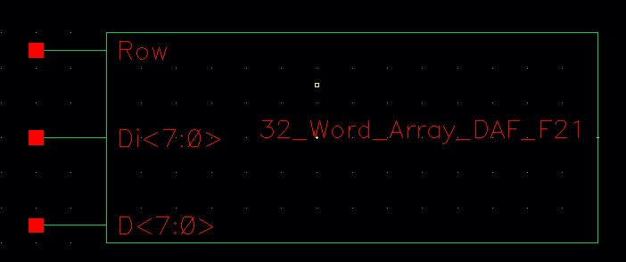
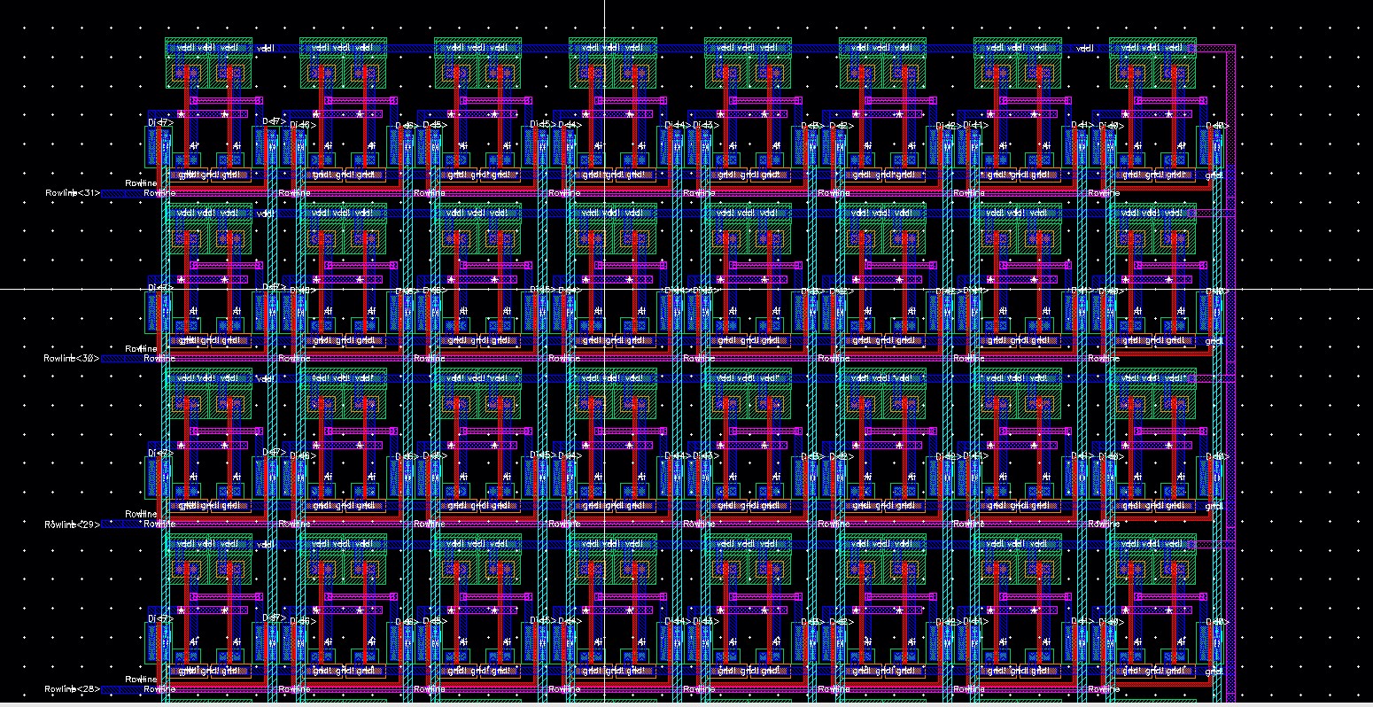
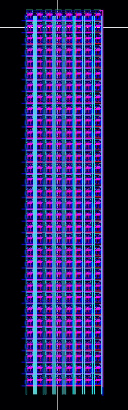
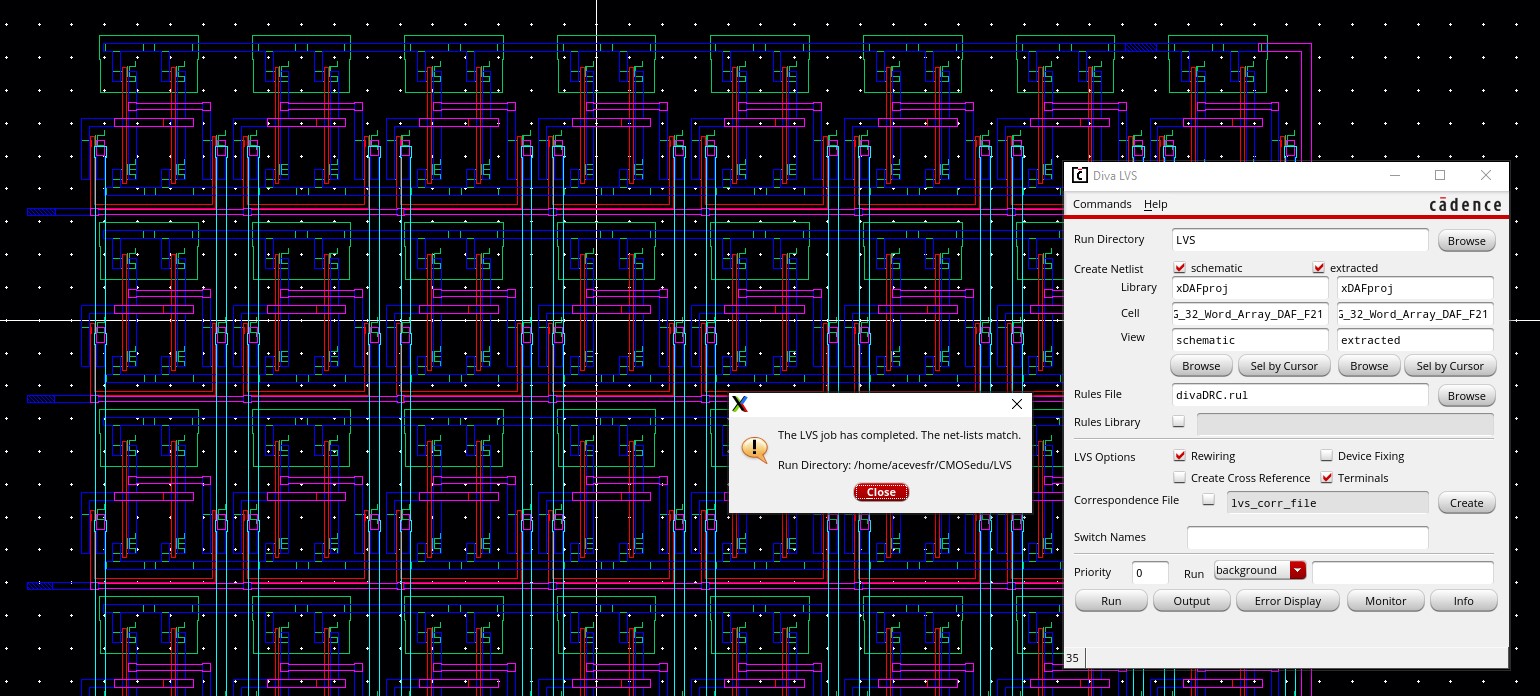
32-bit Word Array
32-Bit word is made from the 8-bit SRAM
Symbol
Layout
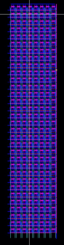
close up
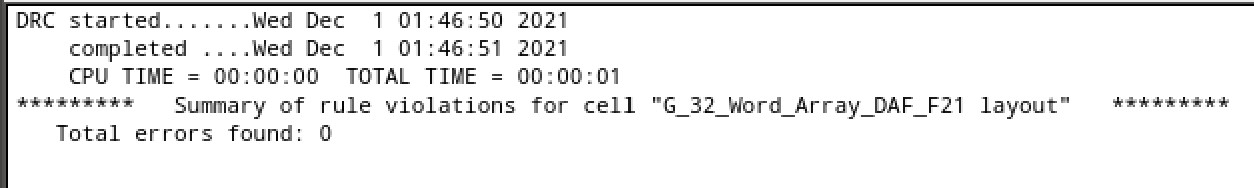
DRC
Extract
LVS
SIM 32-bit Word Array
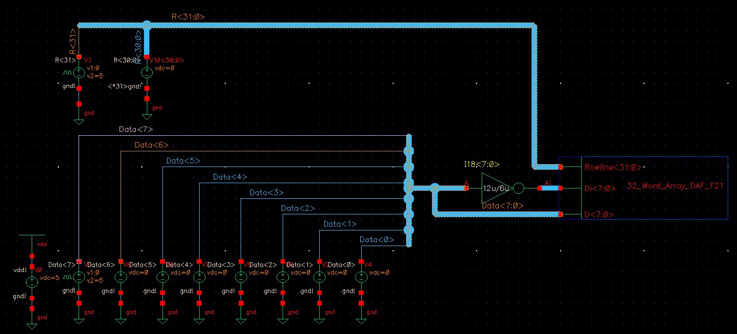
Simulation works
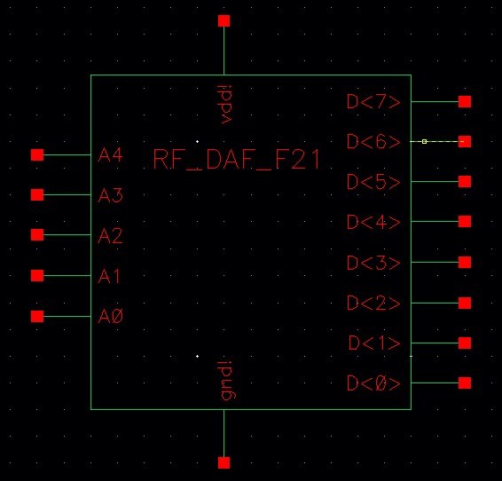
Register File
Symbol
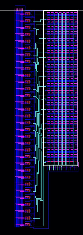
Layout
DRC
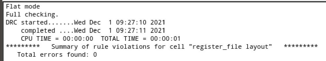
Extract and LVS
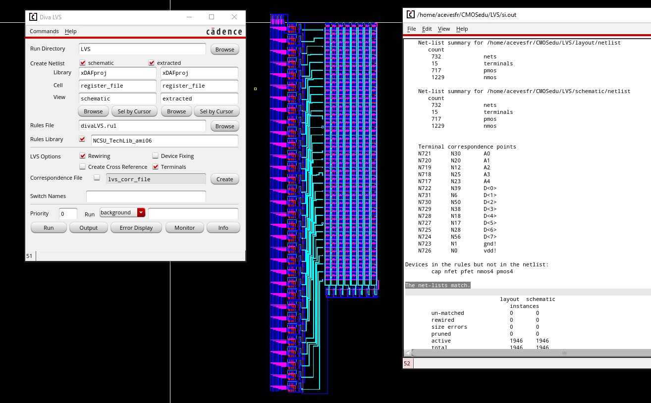
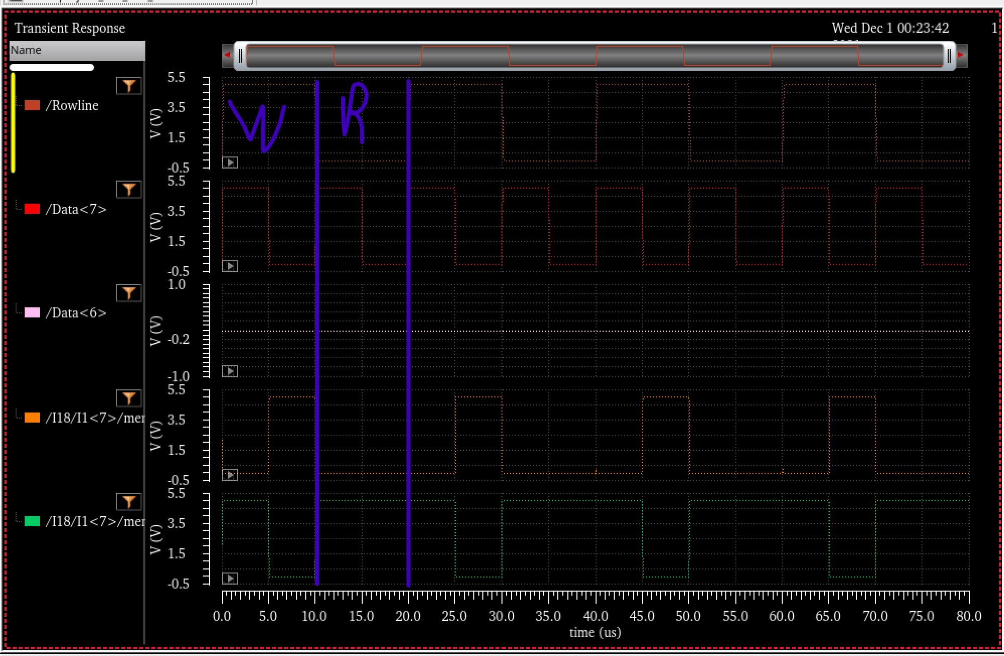
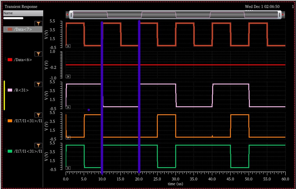
Register File SIM
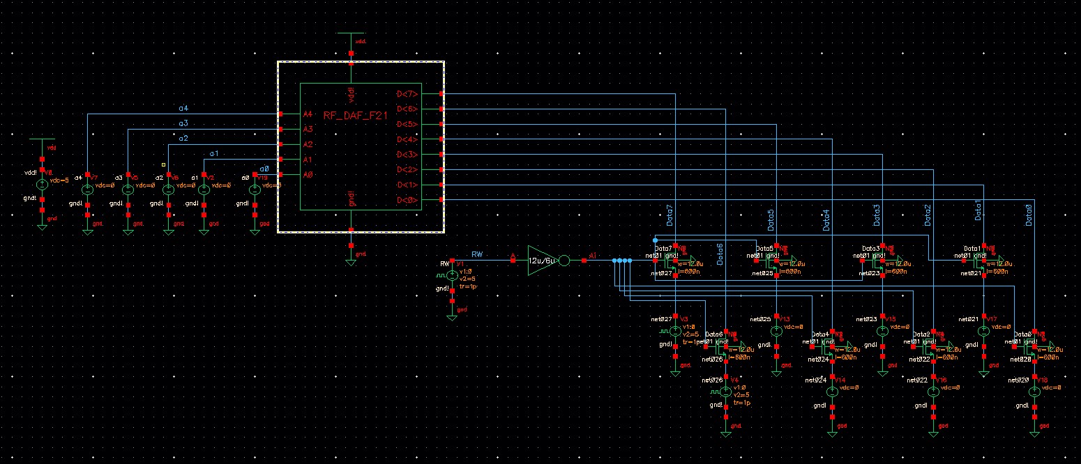
OUTPUT
The following screenshots shows the simulation setup/results of the Register File. Setup accessing address 00001.
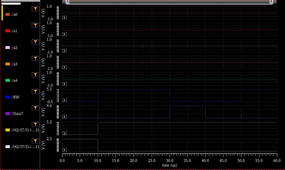
Conclusion
This concludes the RF project usesing a 5-bit
address
to access the 32 8-bit words.
END of Project
for ZIP Request via email.
Return to Labs