Lab 2 - EE 421L Digital Integrated Circuit Design, Fall 2020
Author: William Wherry
Email: wherrw1@unlv.nevada.edu
9/2/2020
Lab
description:
In this lab we'll use n-well resistors to implement a 10-bit DAC.
Our design is based upon the topology seen in Fig. 30.14, below, in the CMOS book.
Prelab work:
- Prior to coming to lab make sure you understand how the input voltage, Vin, is related to B[9:0] and Vout (the quiz may ask a question about this).
- In your lab report: 1) provide narrative of the steps seen here,
2) provide, and discuss, simulation results different from the link to
illustrate your understanding of the ADC and DAC, 3) explain how you
determine the least significant bit (LSB, the minumum voltage change on the ADC's input to see a change in the digital code B[9:0]) of the converter. Use simulations to support your understanding.
- Backup your webpages and design diretory.
First,
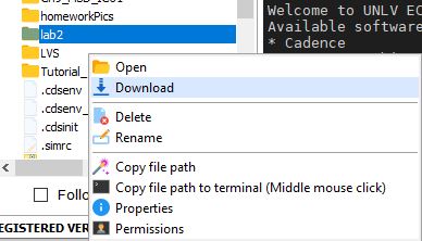
we had to upload lab2.zip to our CMOSedu directory by either uploading
the .zip file first, or unzipping the file first, then uploading the
resulting folder. I unzipped it first, then uploaded it. Next you have
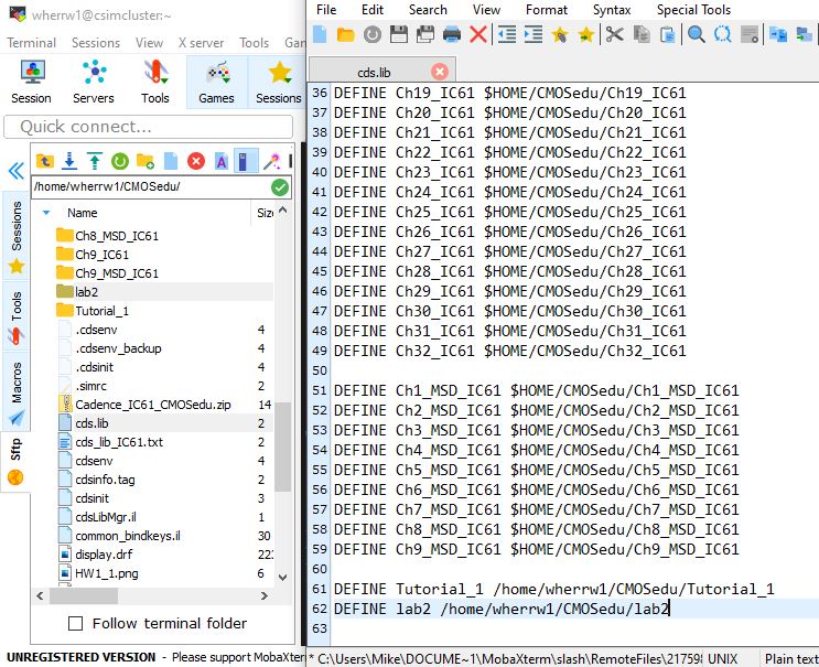
to point the cds.lib file at the new lab2 folder, because it is going
to be used as a Cadence library. You do this by adding $HOME/CMOSedu/lab2 to your cds.lib file on a new line, as seen below.
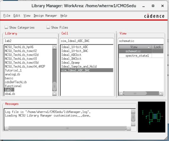
Next,
we open Cadence using either MobaXterm or through the terminal in our
VNC and navigate to our new library in the Library Manager. We select
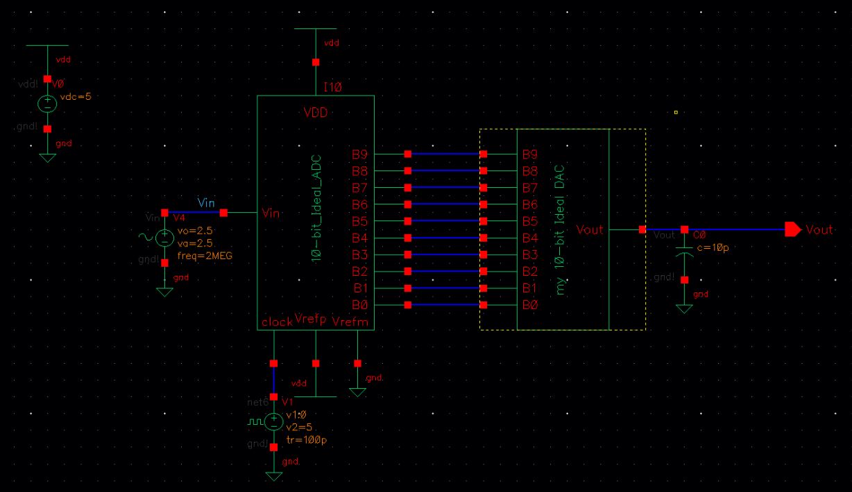
the lab2 library, then "sim_Ideal_ADC_DAC", then open the schematic.
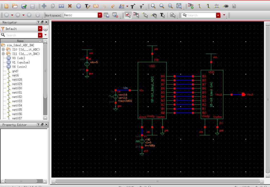
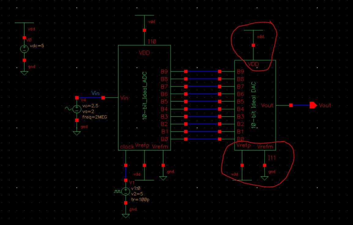
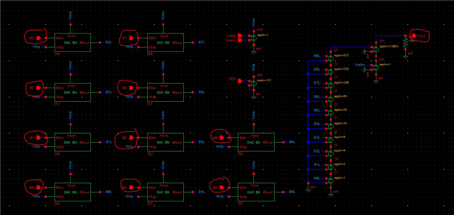
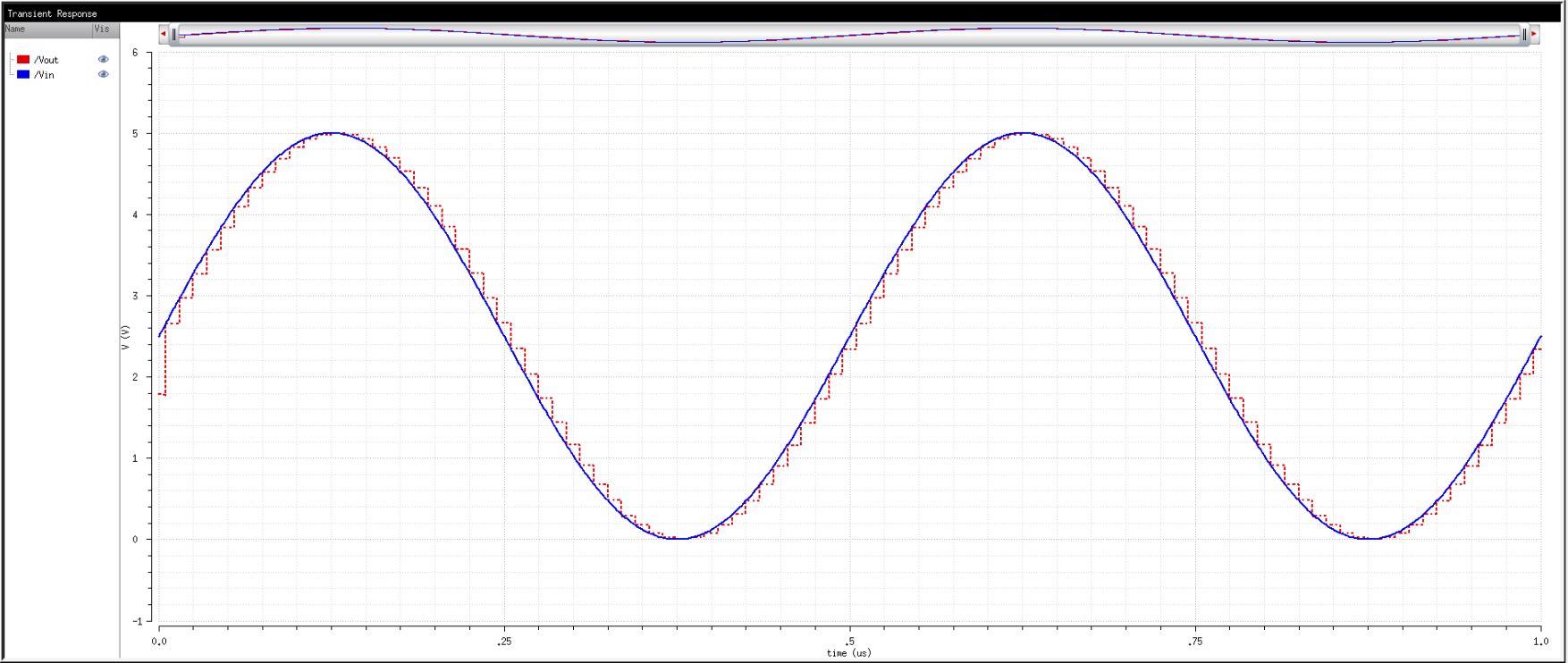
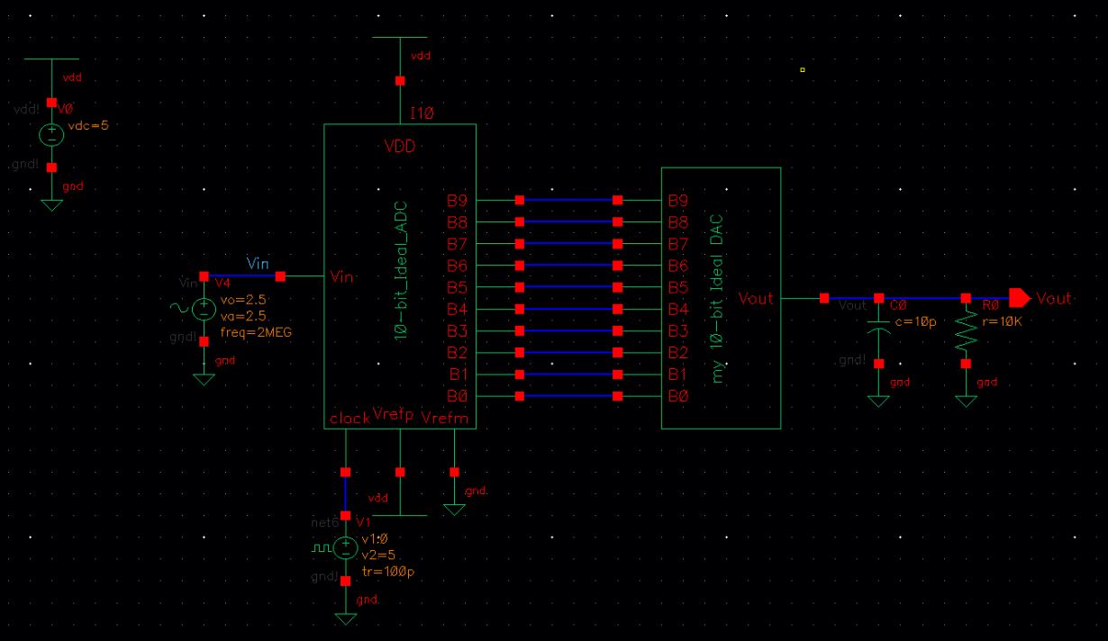
Once the schematic is open you will see the Digital-to-Analog to Analog-to-Digital converter pictured below.
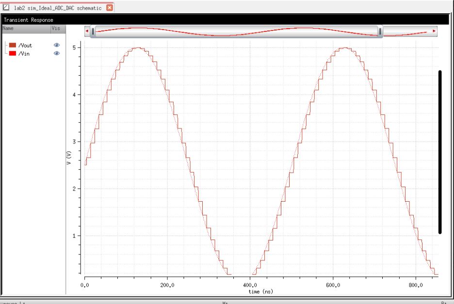
From
here on I wanted to test the capabilities and properties of the device
in the schematic, so I changed the input voltage and observed what
happened in the simulation. Since this is a 10-bit ADC, it should
follow the formula of VDD/2^N = Least significant bit and considering
that our VDD = 5V, that means 5V/2^10 = 4.88mV. That should be the
minimum voltage input required to see a change in the digital code in
our graphs. Below are the results of my observations.
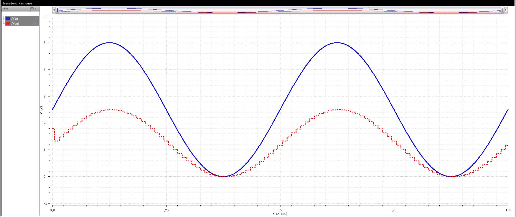
Graph 1 - Default Inputs:
Vin: 2.5V
DC Offset: 2.5V
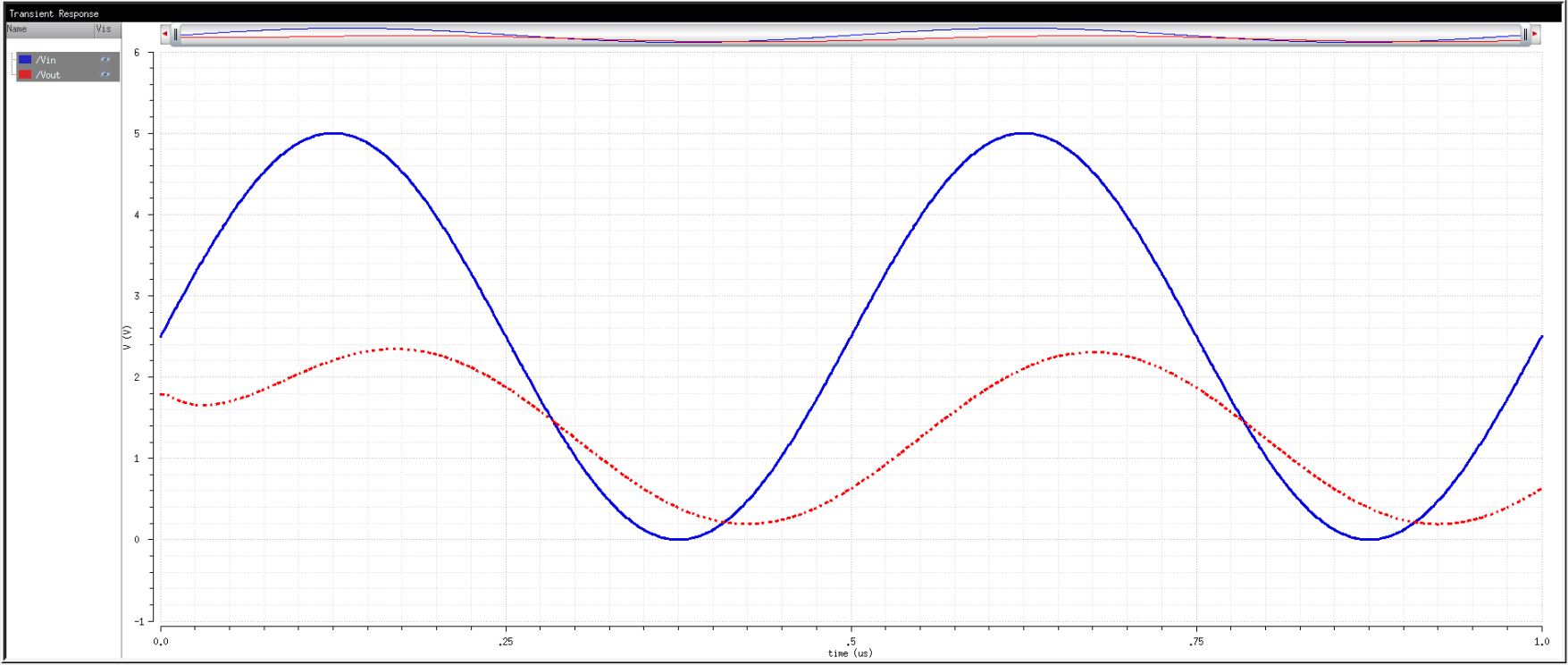
Graph 2 -
Vin: 2.0V
DC Offset: 2.5V
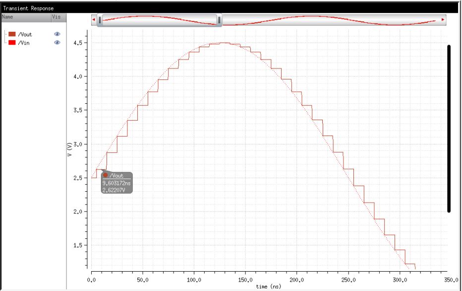
Graph 3 -
Vin: 1.0V
DC Offset: 2.5V
Graph 4 -
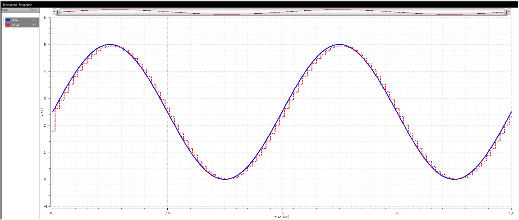
Vin: 0.01V
Dc Offset: 2.5V
In graph 4 the difference
between 0V input (ignoring the
DC offset) and the plataeu of the first rise in voltage is almost
exactly 4.88mV, the same as what I calculated using the formula
earlier; the minimum input required to get a change in the digital code
in our graphs.
You
can see from the graphs part of the story of what is happening with
these two devices linked up the way they are. The ADC gets an input
(Vin) analog signal and converts it to a digital (binary 10-bit,
B[9:0]) signal, which basically means that a continuous signal is
turned into a discrete signal. Then that discrete signal is "smoothed
out" into a continuous analog signal again by the DAC. You can see the
result of this as the smooth Vin signal gets turned into a jagged Vout
signal, but the output is roughly the same in amplitude and
shape. The number of bits affects the resolution, which affects
how many times the signal is divided up in a given cycle. More bits
would allow the ADC to respond to smaller signals than the 4.88mV
minimum we calculated.
Backing up work:
As always, we must practice backing up our labs and website directory by zipping up our files and emailing them to ourselves.
Main Lab Content:
- The design of a 10-bit DAC using an n-well R of 10k
- The 2R resistor should be implement with two separate 10k resistors in series
- How to determine the output resistance of the DAC (answer: R) by combining resistors in parallel and series.
- Delay, driving a load
- Ground
all DAC inputs except B9. Connect B9 to a pulse source (0 to VDD) and
show, and predict using 0.7RC, the delay the DAC has driving a 10 pF
load
- Verify the simulation results match your hand calculations
- How
to create a symbol view for your design with the exact same footprint
as the Ideal_10-bit_DAC symbol view.
- Simulations to verify your design functions correctly.
- In a real circuit the switches seen above (the outputs of the ADC) are implemented with transistors (MOSFETs).
- Discuss what happens if the resistance of the switches isn't small compared to R.
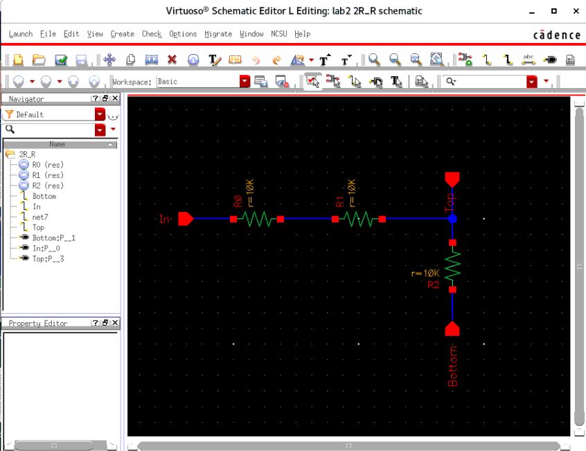
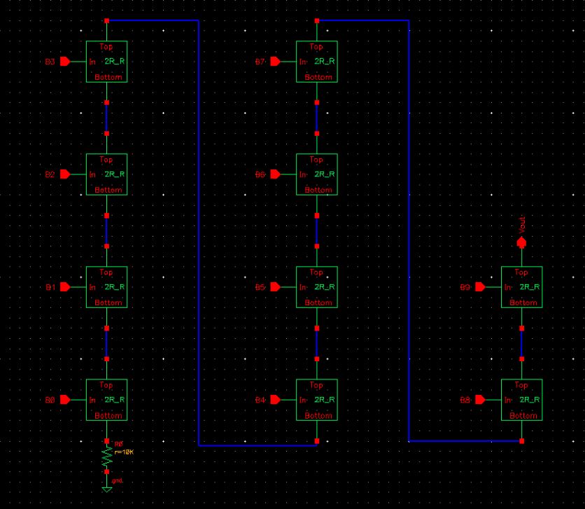
The first step of our journey to creating a 10-bit DAC is to design
a reusable voltage divider using 10k n-well resistors. Normally, the
divider is made of two resistors, one is 2R and the other is R, but for
our lab we will be using two separate resistors to form the 2R
resistor. First we make a new schematic implementing our three
resistors.
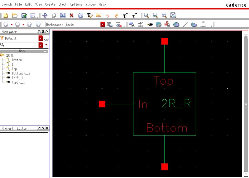
Next,
we have to make a symbol for it, so it can be used as many times as we
need in our DAC. We do this by first setting input/output pins where we
want them to be (making sure to press Q on them and set them to the
correct input or output connectivity), then we select
Create->Cellview->from Cellview to create our new symbol. We can
then make it aesthetically pleasing by adding shapes and moving things
around until we are satisfied. We have to be sure to check and save all
of our work when we are finished.
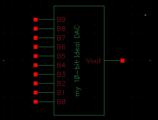
Now
we have what we need to make a DAC. We could make the whole thing from
scratch, but luckily we have an example circuit that we can recycle for
our design. First we have to copy the cell "Ideal_10-bit_DAC" from the
library manager and rename it something we can recognize. Then we can
simply open up that symbol, click on it, and press shift+X to descend
into it. Then we simply delete everything but the pins for the bits and
Vout. Before we do that we should delete the "Vrefm," "Vrefp,"
and VDD pins on the DAC since we will not be using them and they will
cause errors when we gut the internals.
Inside
the copy of the DAC, we want to keep only the circled pins. Everything
else should be deleted so we can replace them with our resistors and
connecting wires.
Since
we are building a resistor-based DAC, we just need to connect our bit
pins to the input of our 2R_R symbol that we created earlier, then
connect each top pin to the bottom pin of the next bit's 2R_R
schematic, with the final bit's 2R_R being connected to Vout at the
top. Also, on the least significant bit's bottom pin we connect another
10k resistor along with a gnd connection.
Hand Calculations:
Finding the output resistance of the DAC:
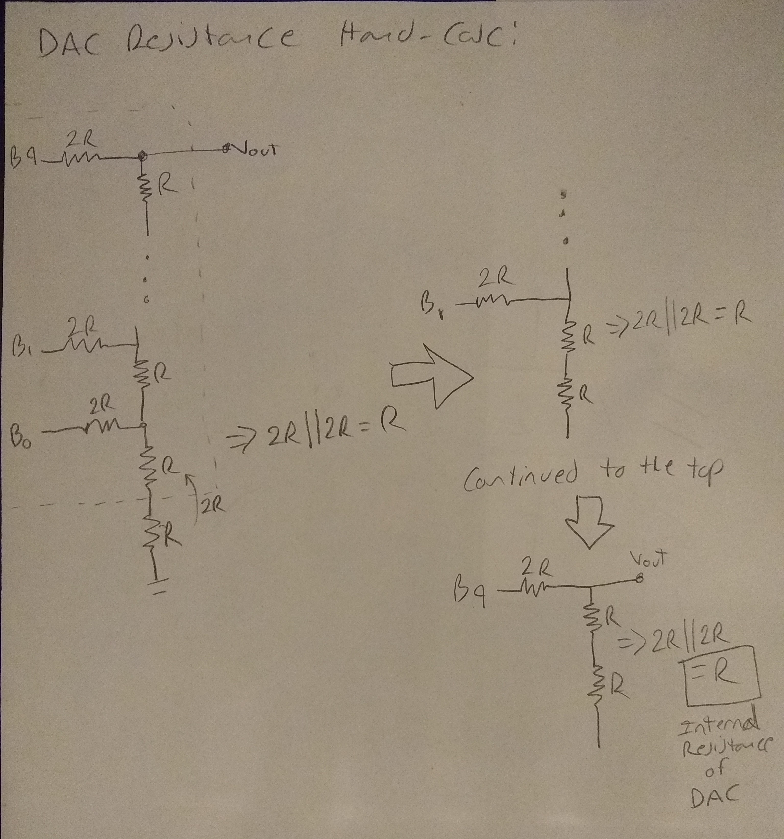
The output resistance of the DAC should be equal to R, which in our case would be R = 10k ohms.
Finding the expected delay when using a 10pF load:
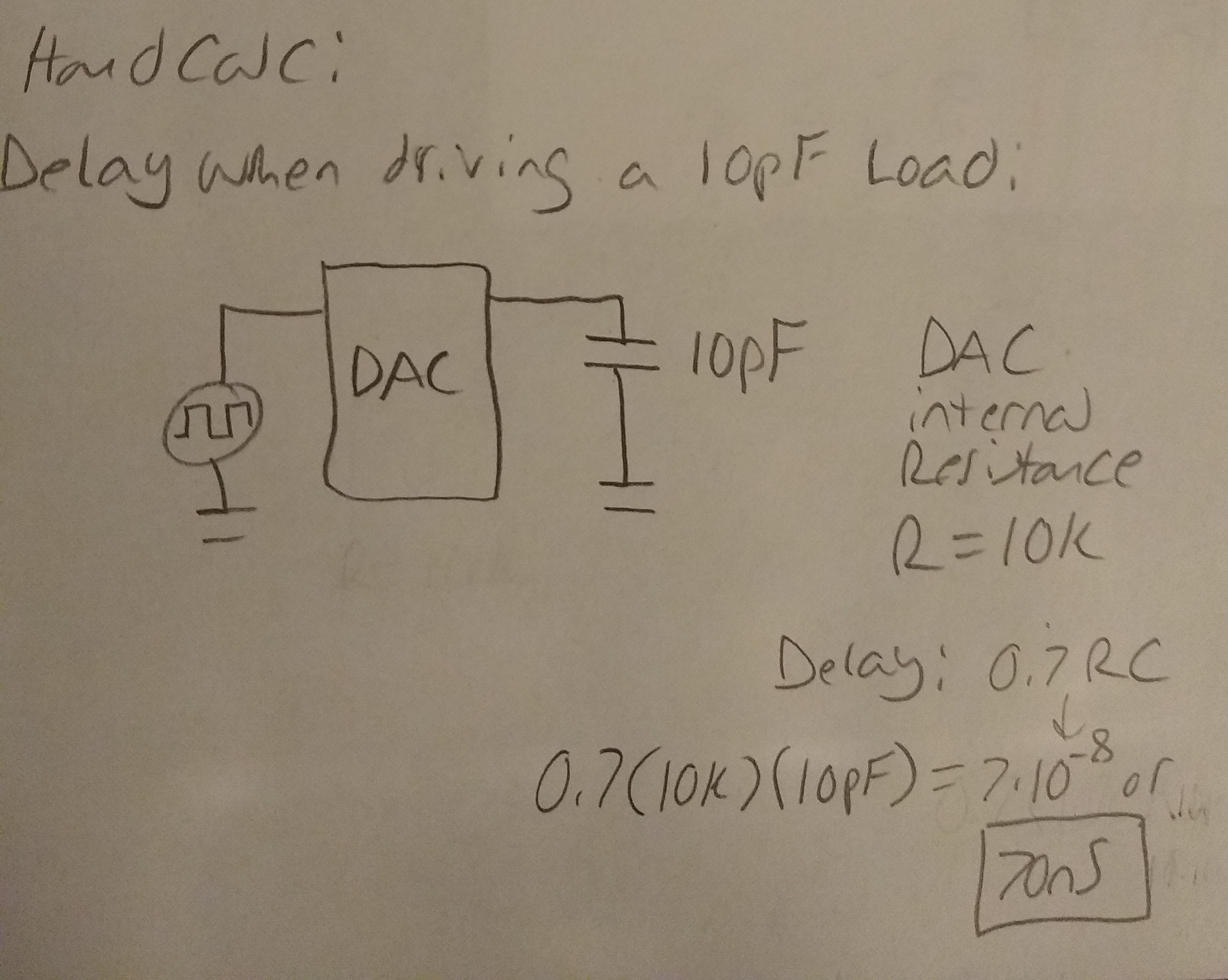
The
expected delay of the output signal when using a 10pF load should be
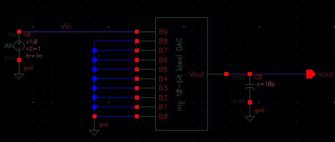
about 70ns. Here we set up the DAC to test if that delay is true or not
by grounding all inputs except b9 and sending a pulse signal through it
with a 10pF load at the output.
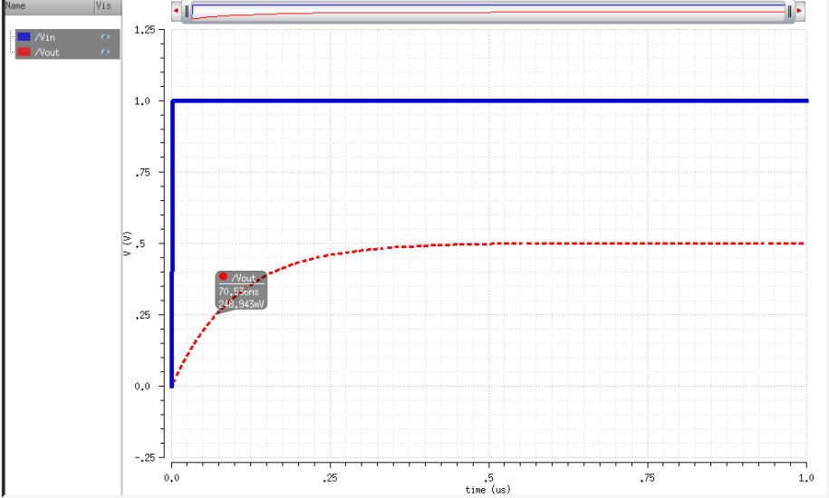
As you can see in my graph, the delay at the 50% output amplitude, td, is at about 70ns just as we calculated.
Testing our DAC in the original circuit:
Now
that we have assembled our DAC, we can replace the original DAC with
ours and see how they compare. We can easily replace the original by
selecting it, pressing Q, and renaming the cell to the name we gave our
copy. We will have to clean up some wires after doing this or the
schematic will throw out errors.
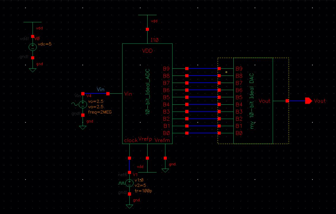
Now
we can open the ADE and simulate the circuit with the same parameters
that were originally used by using load state. When we hit the simulate
button we should have a very similar graph to the original.
As
you can see, our design matches pretty closely with the original and it
simply uses resistors. Now we can see what happens when it drives
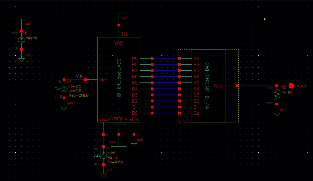
different kinds of loads. First we start by testing only a capacitor at
Vout. We will try a 10pF capacitor and see what happens.
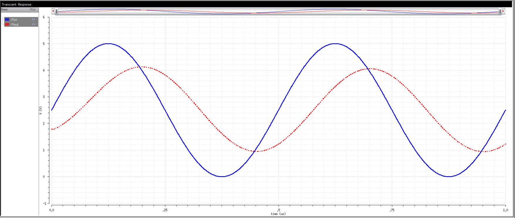
It
looks like a small capacitor load smooths out the jagged edges of our
output caused by the conversion from analog to digital to analog
signals. You can also see that the 10pF capacitor causes the output to be delayed.
Next we will try a resistor only. We will try a 10k resistor, then a large 1M resistor.
10k ohm resistor load:
1M ohm load:
The output
for the 1M resistor is almost the same as it is without a resistor at
all, while the 10k resistor reduces the amplitude of the signal. This
is because the smaller 10k resistor is acting like a voltage divider
with the output resistance (10k ohms) of our DAC, causing the voltage to be split
with that resistance. The 1M resistor is much larger, so it would get
almost all of the voltage anyway and is unnoticable.
Now we will try it with a capacitor and resistor as a load.
From the graph,
you can see that it basically combines the two results that we saw
before. That is, it reduces amplitude of the output via voltage
divider, but also delays the output by about 70ns and smooths out the
waveform a bit.
Based
on these results, we can conclude that our DAC is functional, but we
have to be mindful of any load we want to put on it as a small
resistive load can cause a voltage divider and reduce our amplitude
(unless that is what we want). Using only a resistor or no load keeps
the output signal in phase with the input signal, but adding a
capacitor adds a delay or phase shift to the output which can be
calculated with 0.7RC = delay.
The capacitor can also be used to smooth the output signal if we wish.
These results can be combined if you use a resistor and capacitor load
in parallel.
Additional Question:
- In a real circuit the switches seen above (the outputs of the ADC) are implemented with transistors (MOSFETs).
- Discuss what happens if the resistance of the switches isn't small compared to R.
If
the resistance of the switches is not small, then it would be in series
with the 2R resistance of the DAC and cause a higher output resistance
than the R value that we calculated. That could cause some unintended
effects down the line.
Side Note:
- If you have simulation convergence problems you can force the simulation to converge by going to, in the ADE, Simulation -> Options -> Analog
- Set the values as seen below
- relative tolerance, reltol, of 10% (= 1e-1)
- voltage absolute tolerance, vabstol, of 100 mV (= 1e-1)
- current absolute tolerance, iabstol, of 1 mA (= 1e-3)
- The accuracy of the simulation will, obviously, be degraded
Since
I did not have this issue in my simulations, these instructions were
not used, but it is worth noting in case anyone wants to replicate this
experiment based on my lab report.
Backing up our work:
As always, we must back up our work. First we download our lab2 folder from MobaXterm, then zip it up and email it to ourselves.
With our DAC successfully designed and tested and our work backed up, lab 2 has reached its conclusion.
Return to William Wherry Labs Directory