Final Lab Project- EE 421L Fall 2020
Authored by: Nathan Pina
Email: pinan1@unlv.nevada.edu
Due Date (Schematics/Simulations): 11/18/20
Due Date (Layouts): 11/25/20
Lab description:
Design,
layout, and simulate a digital receiver circuit that accepts a
high-speed digital input signal D and Di (a differential pair connected
to your circuit from, for example, a twisted pair of wires such as in
an Ethernet cable). D and Di are complements so, for example, if D is
5V then Di is 0V and output = 1. Another example, when D is 1V and Di
is 2V
then output = 0. At high-speeds and long distances the
voltages received aren't full digital logic levels (i.e., 5V and 0V),
hence the need to design, and use , a high-speed digital recevier
circuit. Ideally, when D > Di the receiver outputs a 1. When D <
Di the receiver outputs a 0. Base your design on the topology seen in
Fig. 18.23. Try to design for high-speed and low-power. Characterize
your design (in sims) and the trade-offs. For example, show that you
get higher-speed if you use more energy (burn more power). See if you
can get, in this 500 nm process, 250 Mbits/s (a bit width of 4 ns) with
an input voltage difference of, for example, 250 mV (with D and Di
swinging back and forth between 2.75V and 3V,
for one of many
examples, your circuit outputs the correspondingly correct values).
Note that while Fig. 18.23 shows one inverter on the output you may
find, for example, that two inverters work better (at the cost of
power). Use a table to summarize your design's performance.
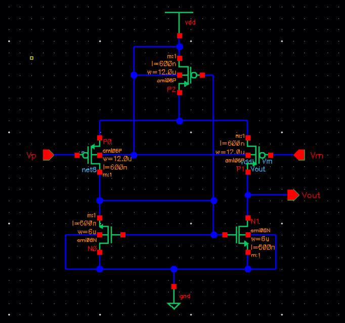
Main Project Design:
The
main design for this digital reciever is based on the designs found in
"CMOS: Circuit Design, Layout, and Simulation", specifically figues
18.23, 18.21, and 18.17. Both the PMOS and NMOS versions of the
self-biasing diff amps were createad and used in order to reduce the
overall delay of the circuit and remove the offset on the output caused
by the Vp and Vm inputs of the reciever. Both of the diff amps were
created using the standard sizes found in the book, 6u/0.6u for the
NMOS and 12u/0.6u for the PMOS. The schematics for both transistors
were created seperately and then combined once there were no errors and
their symbols were created.


NMOS Schematic/Symbol

PMOS Schematic/Symbol
In
additon to the two diff amps, two inverters were also included at the
end of the reciever design to improve logic levels and overall output.
Once all of the components were connected together (2 diff amps, 2
inverters), a final symbol was created for simulation purposes.


Inverter Schematic/Symbol


Digital Reciever Schematic/Symbol
Digital Reciever Simulations:
The
following simulations will test the effeciency of the digital reciever
under various conditions. Initially, the design will be tested with no
load at a frequency of 250 MHz. Once that baseline has been set various
aspects of the design will be changed which includes: load size,
frequency, temperature and VDD voltages. I will also be looking at
the power disappation of the circuit and how it's affected by the input
frequnecy.

1.) Varying Loads

Digital Reciever w/ no load, 250MHz
With no load, the reciever works as expected with the output voltage at VDD (5V) and very good logic levels.

Digital Reciever w/ 1k load, 250MHz
With
a 1k load, the reciever works fairly well as the output voltage reaches
about 2.5V and delay increases slightly above no load conditons.

Digital Reciever w/ 5k load, 250MHz
As
the load increases to 5k, the ouput voltage increases to ~4.3V but
loses some stability at its peak and has it's delay increased again.

Digital Reciever w/ 10k load, 250MHz
At
10k, the ouput voltage continues to increase to a value approaching
VDD. Logic levels still remain differentiable from each other and don't
seem to worsen under bigger loads.

Digital Reciever w/ 20k load, 250MHz
Finally
at a 20k load, the results are similar to the previous two tests. The
ouput voltage increases while still maintaining fairly good logic
levels.
2.) Varying Input Frequency
The
following test will measure how the circuit performs with varying input
frequencies. For testing purposes, both inputs (D and Di) will always
swing back and forth between 2.75V and 3V, but will have their periods
changed. The load will be kept at 1k, which simulates the practical
scenario in which this circuit would function under.


Digital Reciever at 100 MHz
At
100Mhz, the cirucit functions very well. The logic levels are clearly
defined and the peak output voltage in near 2.5V and stable. The bit
width is 4ns or 250 Mbits/s with an input voltage difference of 250mV.

Digital Reciever at 200 MHz
At
200Mhz, the cirucit starts to decrease in stability. The logic levels
and peak voltage are still well-defined but less stable with the peak
being rounded rather than flat. The bit
width also got shorter by decreasing to about 2.6n or ~380Mbits/s which
is faster but costs the circuit stability and power consumption.

Digital Reciever at 500 MHz
Jumping
up to 500Mhz, the circuit starts to lose all functionality. The logic
levels are not clearly defined and the ouput voltage does not even
reach 2.5V. Although this is much faster than the previous tests, the
circuit will not work as intended and has reached its limit in terms of
input frequnecy.
3.) Varying VDD Voltages
The
following simulations will test limits of the cirucit in terms of its
VDD voltage. VDD will swept from 2-5V while maintaing a 1k load and
250Mhz input frequnecy.

Digital Reciever at 5V VDD
At 5V, the circuit functions as expected like in previous simulations. This will be our baseline.

Digital Reciever at 4V VDD
At
4V, the ouput voltage starts to decrease by a significant amount. The
logic levels start to become less pronounced and the waveform as a
whole becomes a lot more "rounded".

Digital Reciever at 3V VDD
Once
we reach 3V the circuit starts to lose most of its functionality. The
ouput voltage is way below its intended target of 2.5V and the logic
levels are not usable.

Digital Reciever at 2V VDD
At
2V the reciever stops working and has reached the lower limit of the
VDD voltage. From these results, the ideal VDD voltage for this circuit
is in the 4-5V range with anything lower requiring significant changes
to the overall cirucit design.
4.) Varying Temperature
The
following simulations will test limits of the cirucit in terms of
its temperature. The temp will be swept from 0-100C at 25 degree
increments while maintaing a 1k load and 250Mhz input frequnecy.


From
the simulations above, as the temperature increases the ouput voltage of
the cirucit will decrease. However, this does not significantlly change
the quality of the logic levels or increase the delay time.
4.) Power Calculations at Varying Frequencies
The
following simulations will measure the power dissipation of the cirucit
at varying input frequencies while maintaing a 1k load. This was done
using the built-in Cadence simulation tools.

Digital Reciever Power at 100Mhz

Digital Reciever Power at 200Mhz

Digital Reciever Power at 250Mhz
From
the simualtions above, it is clear that as the frequnecy increases, the
amount of power being dissipated also increases. Although the peak
remains at about 22mW for all tests, the frequency at which this power
is dissipated increases drastically.
In order reduce this, the
obvious solution would be to reduce the frequency at the cost of
overall cirucit speed. You could also use less inverters or improve
upon the design of the diff amps by changing the sizes of the
MOSFETs used.
Main Project Design (Layouts):
The following layouts (including their DRC/LVS tests) will be shown:
- NMOS Differential Amplifier
- PMOS Differential Amplifier
- Inverter
- Digital Reciever
The
NMOS/PMOS diff amps and inverter were laid out first and seperately to
ensure that they DRC and LVS properly. Once they passed both tests,
they were combined to form the main digital reciever layout.


Inverter (DRC and LVS layout)


NMOS Differential Amplifier (DRC and LVS layout)


PMOS Differential Amplifier (DRC and LVS layout)


Digital Reciever (DRC and LVS layout)
Final Design Directory:
lab_proj_NP.zip