Lab 4- EE 421L Fall 2020
Authored by: Nathan Pina
Email: pinan1@unlv.nevada.edu
Due Date: 9/23/20
Lab description:
IV characteristics and layout of NMOS and PMOS devices in ON's C5 process
Pre-Lab:
1) Back-up all of your work from the lab and the course.
2) Read through this lab before starting it.
3) Go through Tutorial 2 seen here.
4)
In the simulations in this lab the body of all NMOS devices (the
substrate) should be at ground (gnd!) and the body of all PMOS devices
(the n-well) should be at a vdd! of 5V.
The majority of
the pre-lab was spent completing tutorial 2 by creating a
schematic and layout for an NMOS and PMOS. Once those are created, we
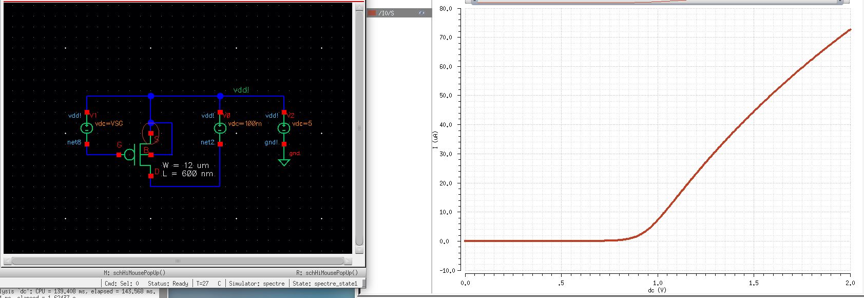
were also asked to simulate the IV curves of ID vs VGS/VSG.
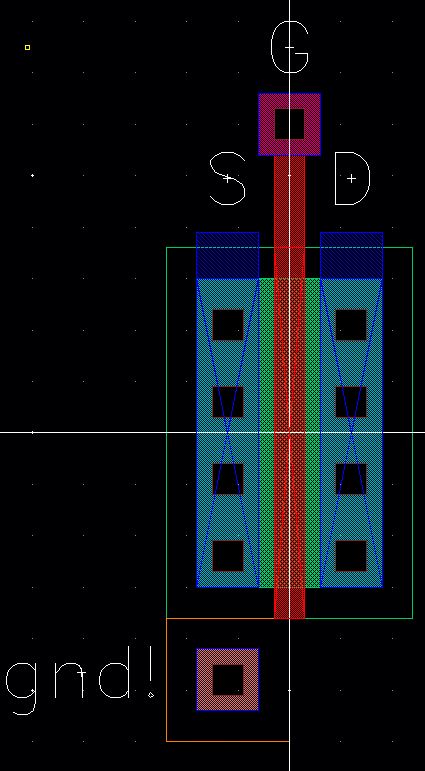
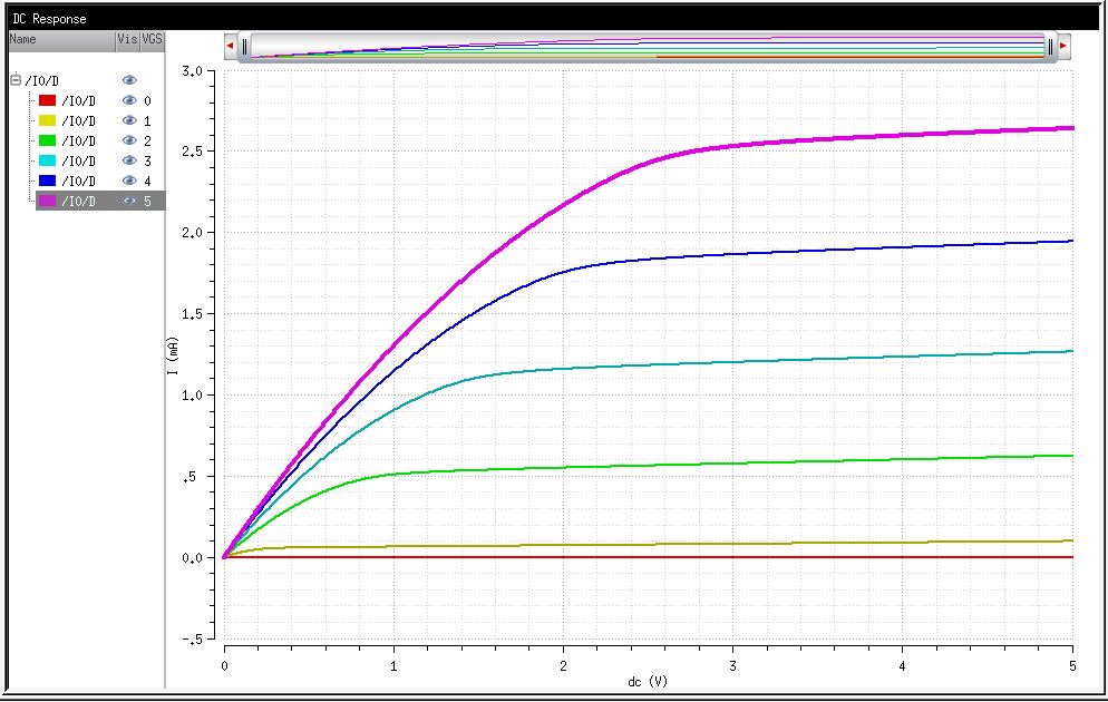
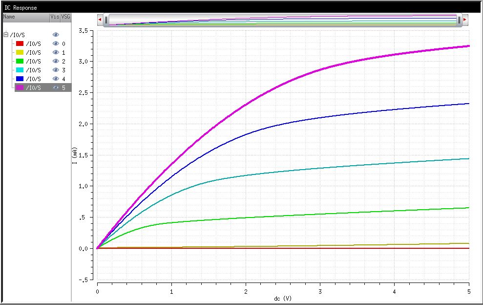
Above are the NMOS layout design and corresponding IV curve.
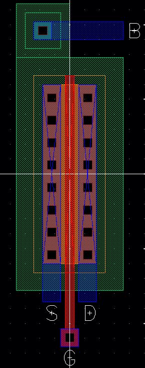
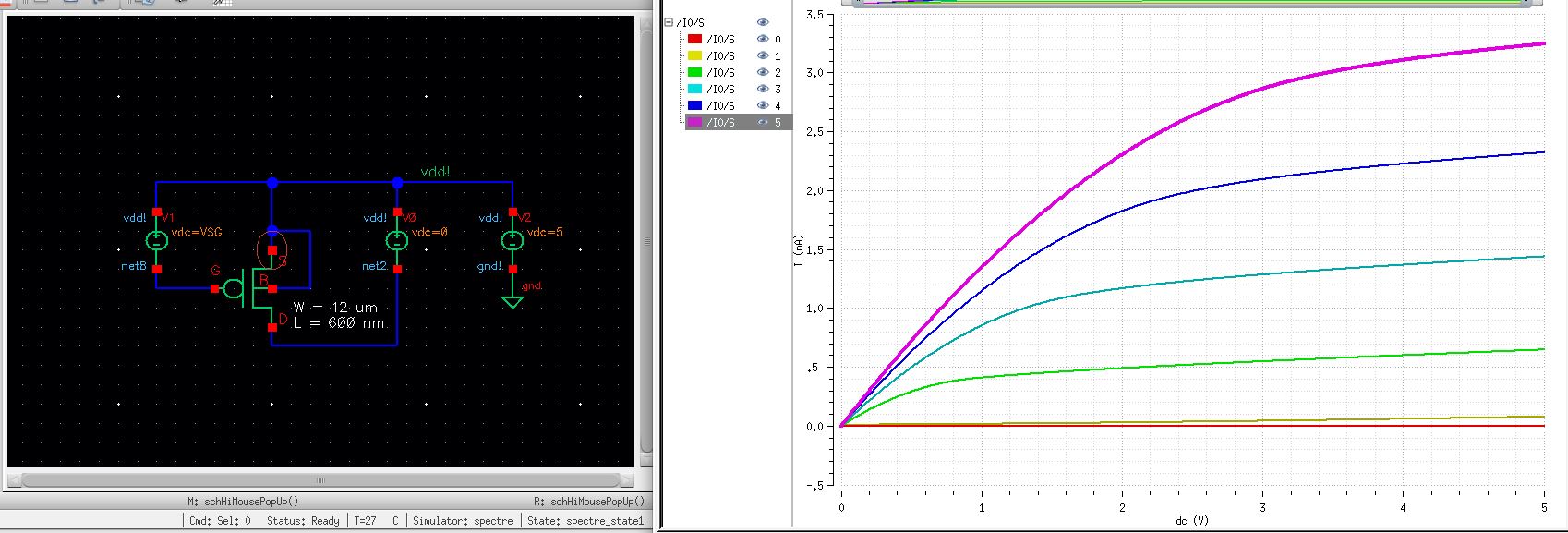
Above are the PMOS layout design and corresponding IV curve.
**THE BODY OF ALL NMOS DEVICES ARE AT GROUND (gnd!) AND ALL PMOS DEVICES ARE AT VDD (vdd!)
Main Lab Work:
The lab is split into two main sections:
a.) Schematics and simulations of IV curves for both the PMOS and NMOS design
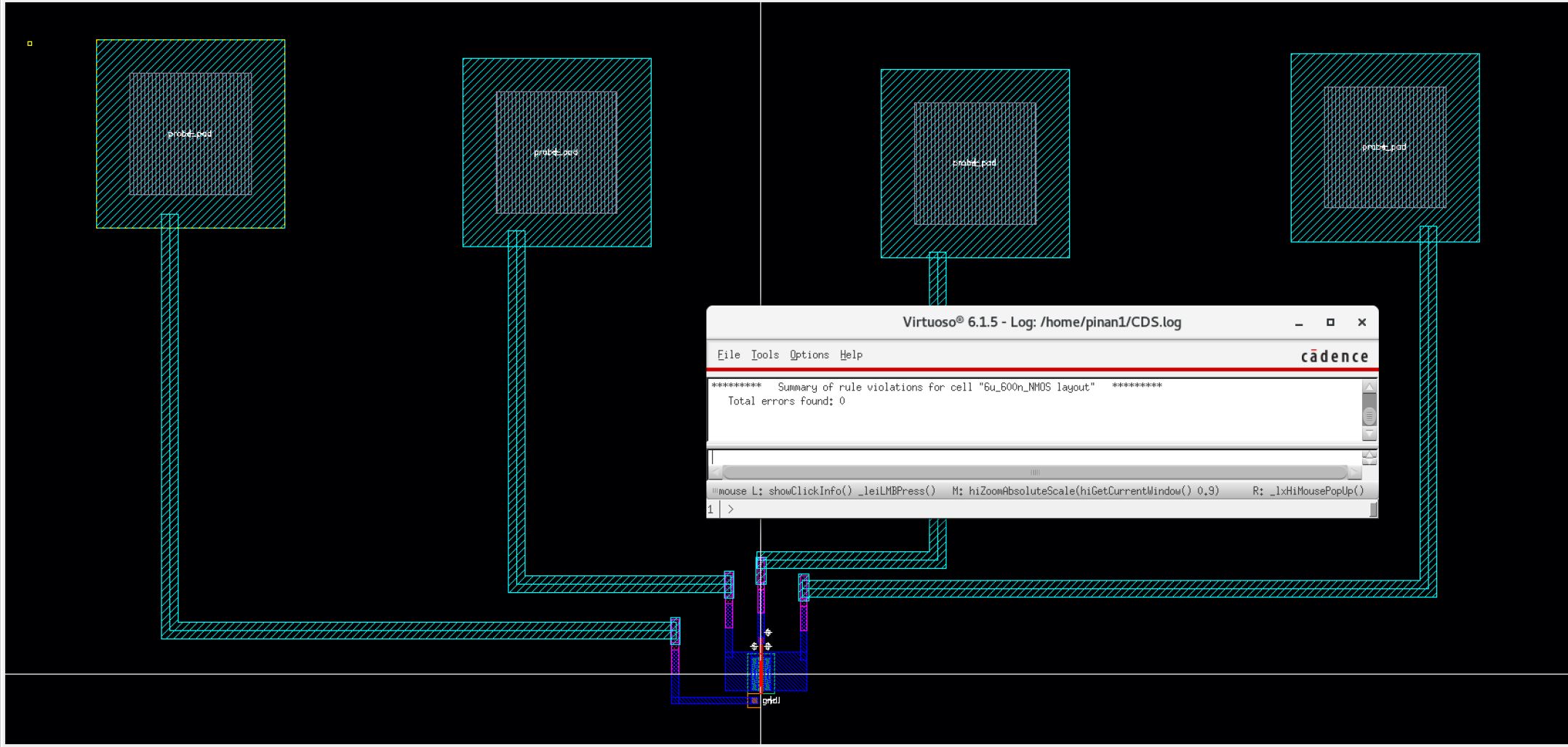
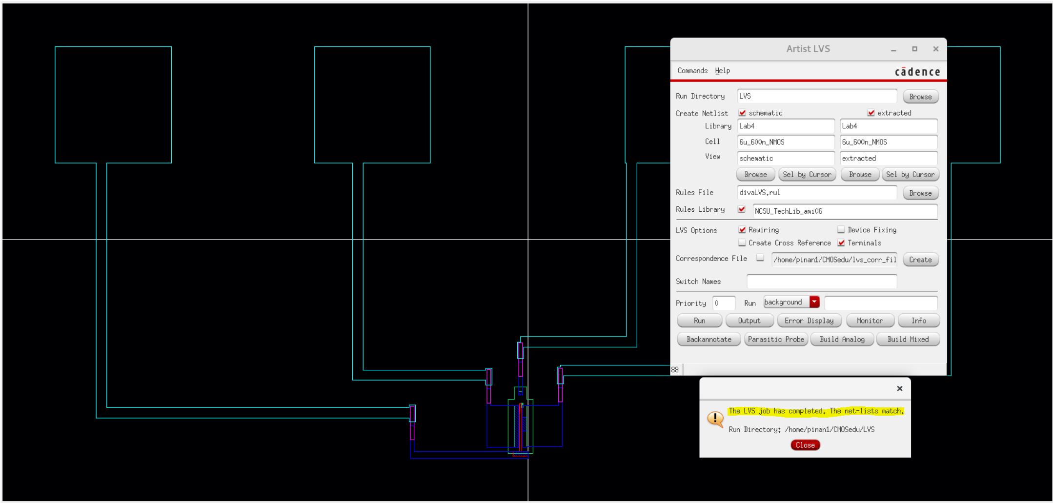
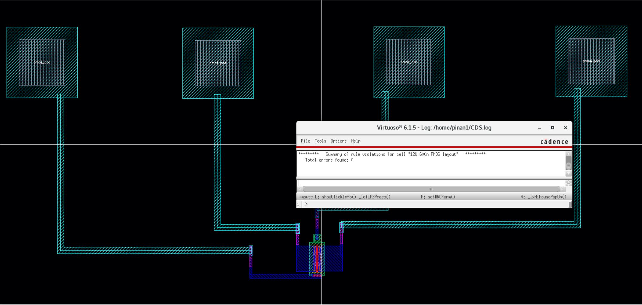
b.) DRC and LVS checks of both devices when all terminals are connected to probe pads
1.) IV Curve Schematics and Simulations
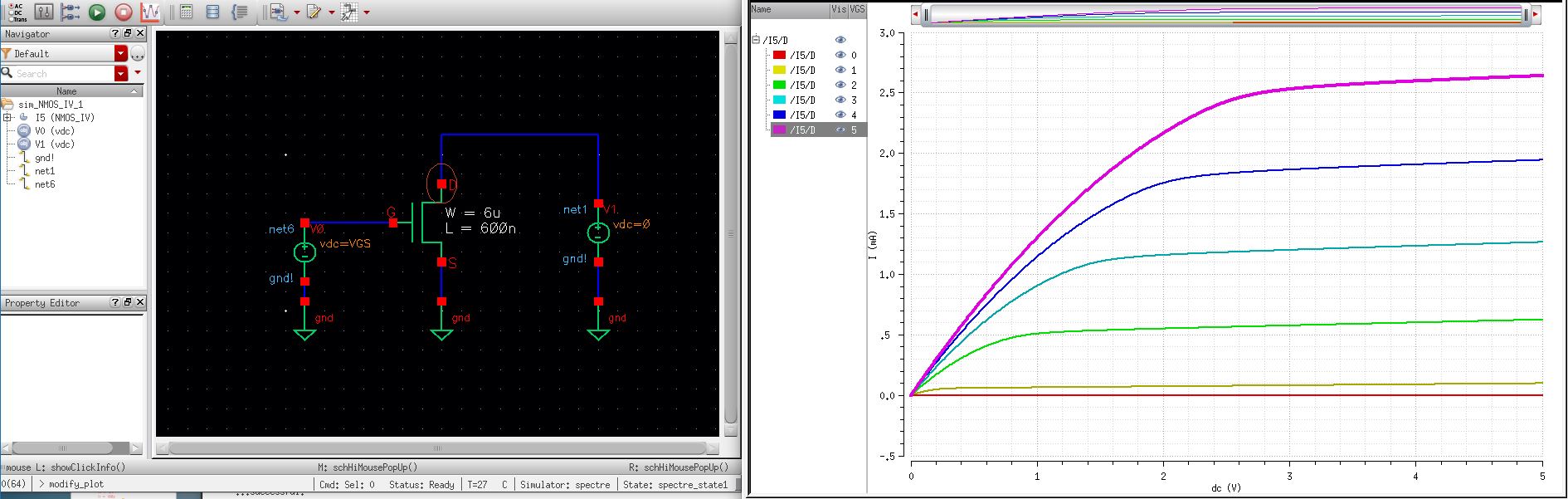
NMOS: ID vs VDS
- VGS varies from 0-5V in 1V steps
- VDS varies from 0-5V in 1mV steps
- 6u/600n width-to-length ratio
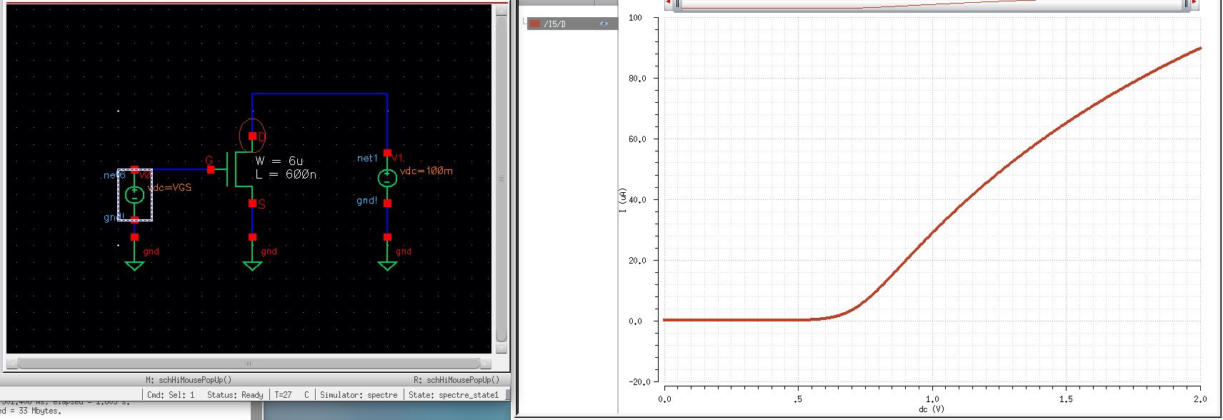
NMOS: ID vs VGS
- VGS varies from 0-2V in 1mV steps
- VDS set to 100mV
- 6u/600n width-to-length ratio
PMOS: ID vs VSD
- VSG varies from 0-5V in 1V steps
- VSD varies from 0-5V in 1mV steps
- 12u/600n width-to-length ratio
PMOS: ID vs VSG
- VSG varies from 0-2V in 1mV steps
- VSD set to 100mV
- 12u/600n width-to-length ratio
2.) DRC/LVS Checks for Layout Designs
NMOS: 6u/0.6u
- Layouts
were created by connecting the probe pads to each of the four MOSFET
terminals through the metal3 layer. Vias were also used to connect the
metal1 layers set on top of the gate, drain, and source to the metal2
connections. Below will be images of the DRC check and the LVS check on
the layout and extracted views respectively.
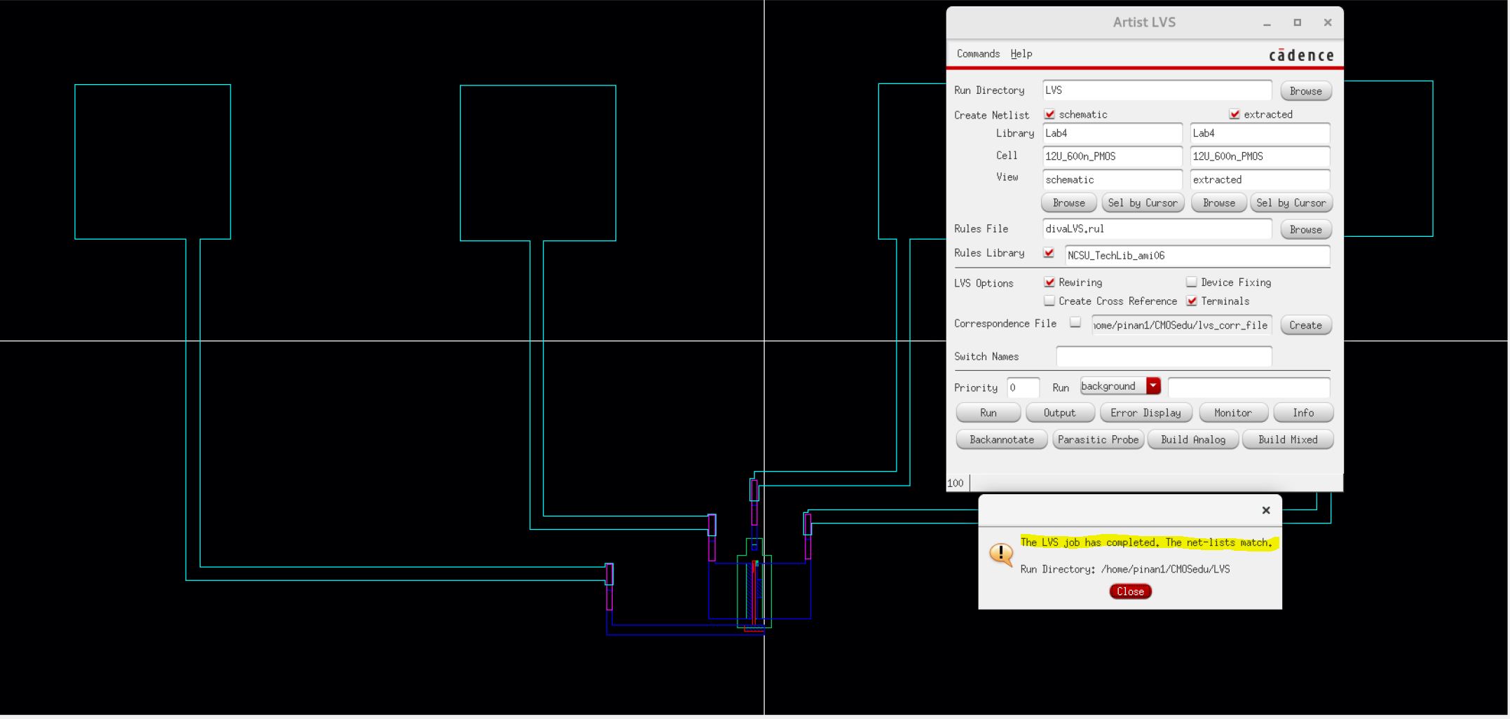
PMOS: 12u/0.6u
- Layouts
were created by connecting the probe pads to each of the four MOSFET
terminals through the metal3 layer. Vias were also used to connect the
metal1 layers set on top of the gate, drain, and source to the metal2
connections. Below will be images of the DRC check and the LVS check on
the layout and extracted views respectively.
Lab Backup
After
I completed this lab, I made sure to back up all files (schematics,
simulations, screenshots etc.) into a zip file and upload to my Google
Drive.