Lab 2 EE 421L
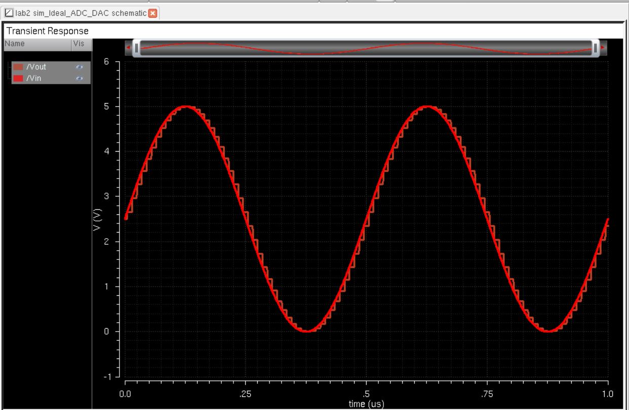
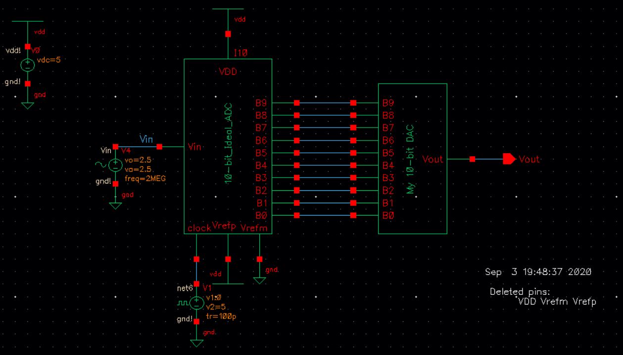
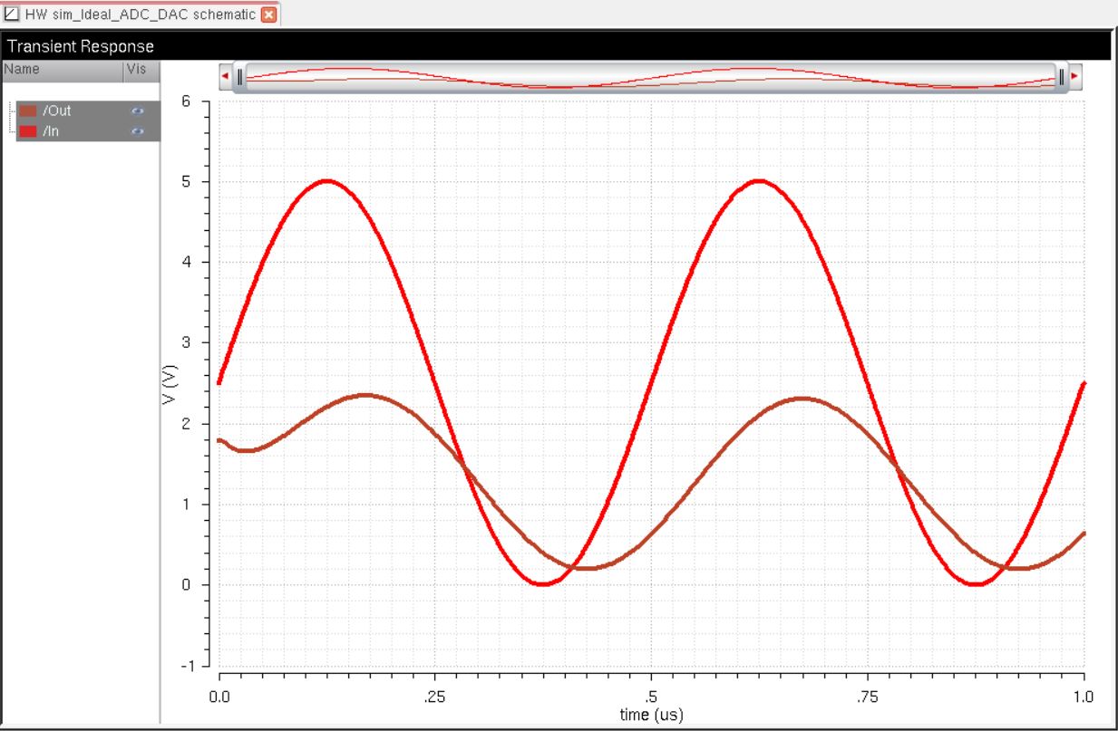
How is Vin related to B[9:0] and Vout?
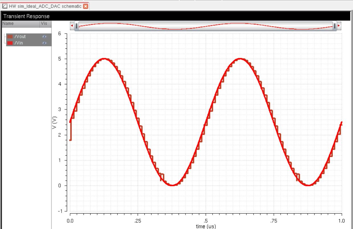
Vin is related to B[9:0] by 10-bit representation of the source, B[9:0] represents a different digit of the 10 bit binary. B9 being the most significant bit, while B0 is the least significant bit. The ADC takes in the analog signal, then converts the signal into a digital signal (waveform with binary coding). After the signal is converted to a digital signal, then the digital signal is recieved by the DAC, which then converts the binary coding from the input and outputs the analog waveform. The way the graph looks is determined by the amount of bits we used, so the more bits the more accurate.
How to determine the Least Significant Bit (LBS)?
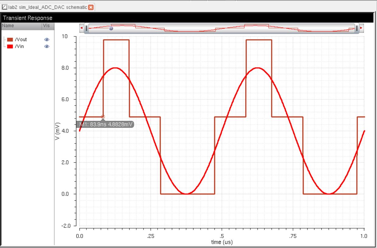
LSB = VDD/(2^n) = 5/(2^10) = 4.88mV
VDD = Input Voltage = 5V
n = Amount of Bits = 10
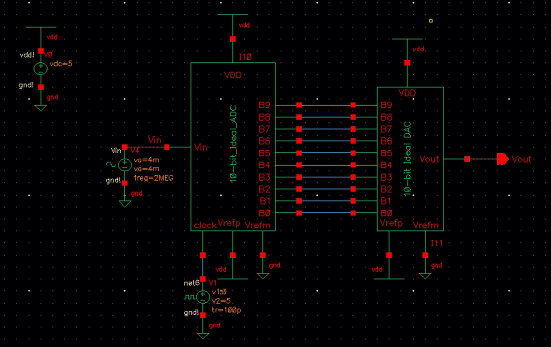
Slightly modifying the sim_ideal_ADC_DAC circuit to 4mV offset and 4mV amplitude, while keeping everything the same to see the least significant bit (LBS).
The simulation above reads 4.8823 mV therefore comfirming that our calculation of LBS is correct.
_________________________________________________________________________________________________________________________
Lab Work
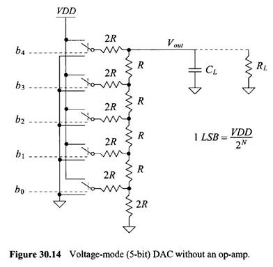
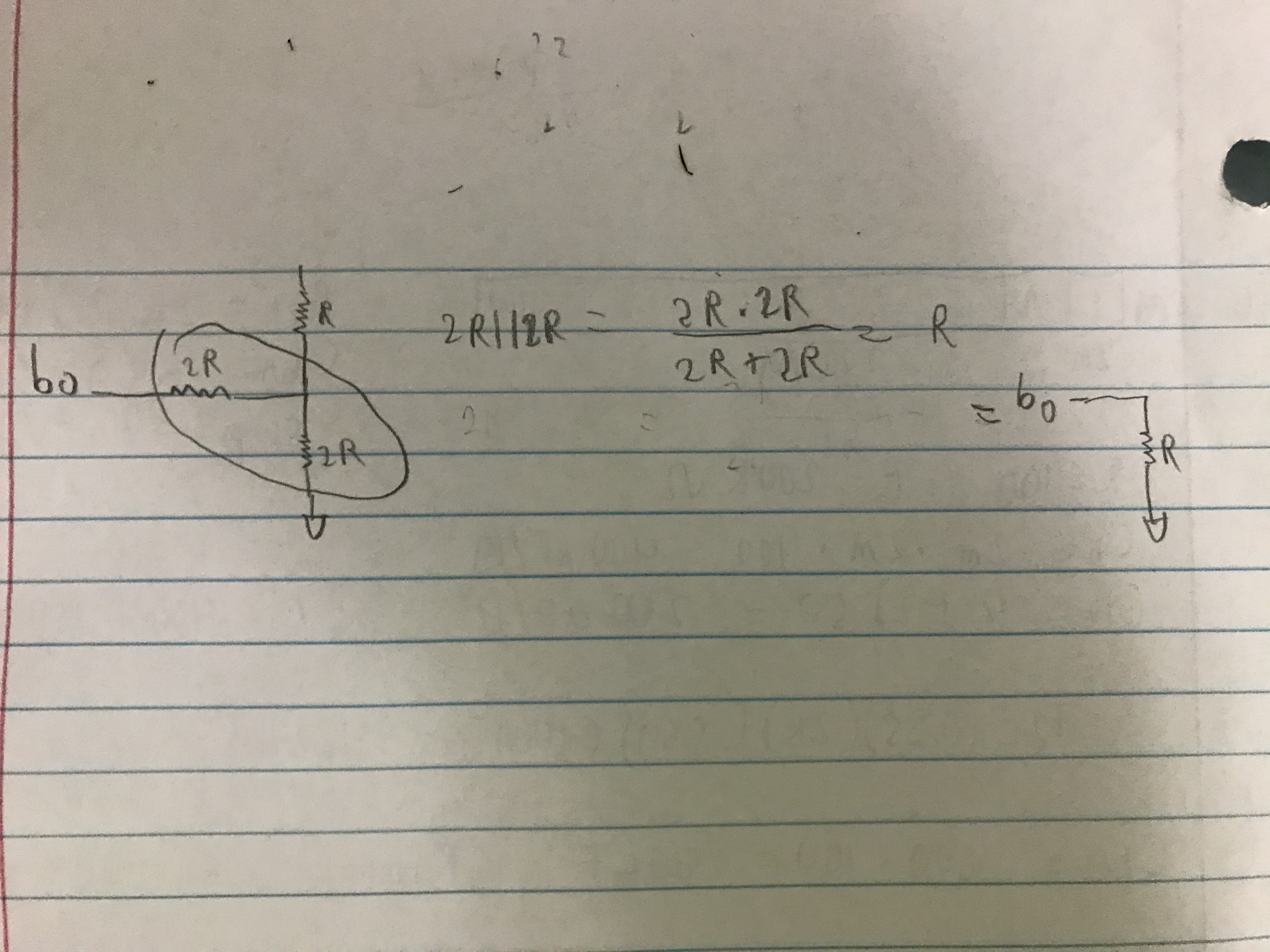
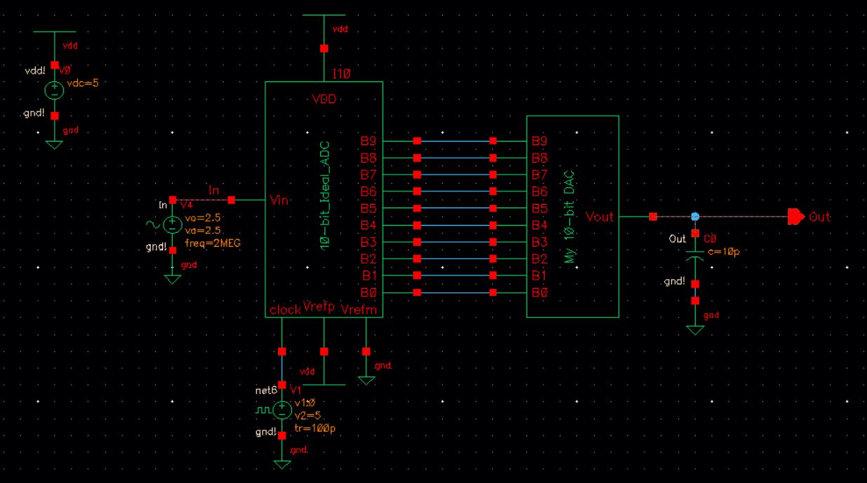
In this lab, we will be using n-well resistors to recreate the 10-bit DAC without op-amp similar to the figure shown below.
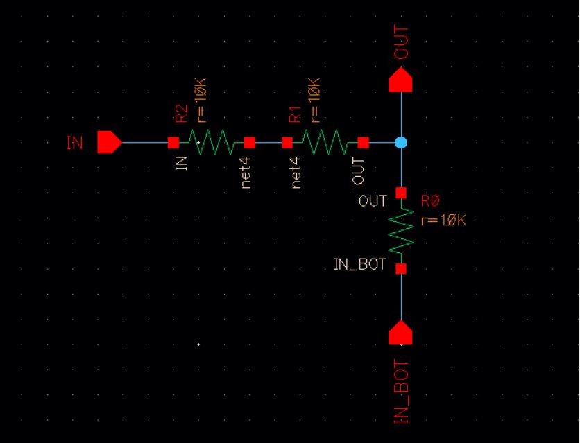
In Cadence we created the 2R and R voltage divider like the figure shown above, but for the 2R we used two resistors in series. After that we turn that into a symbol.
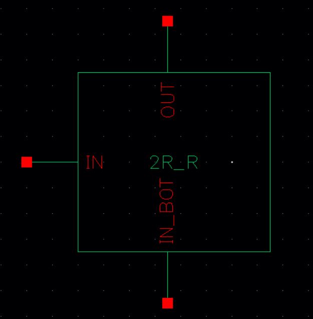
Creating a symbol by going to Create > Cellview > From Cellview
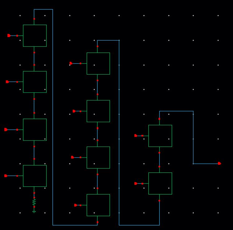
By modifying Ideal_DACbit schematic using the symbol created above and creating a symbol out of it.
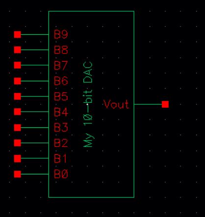
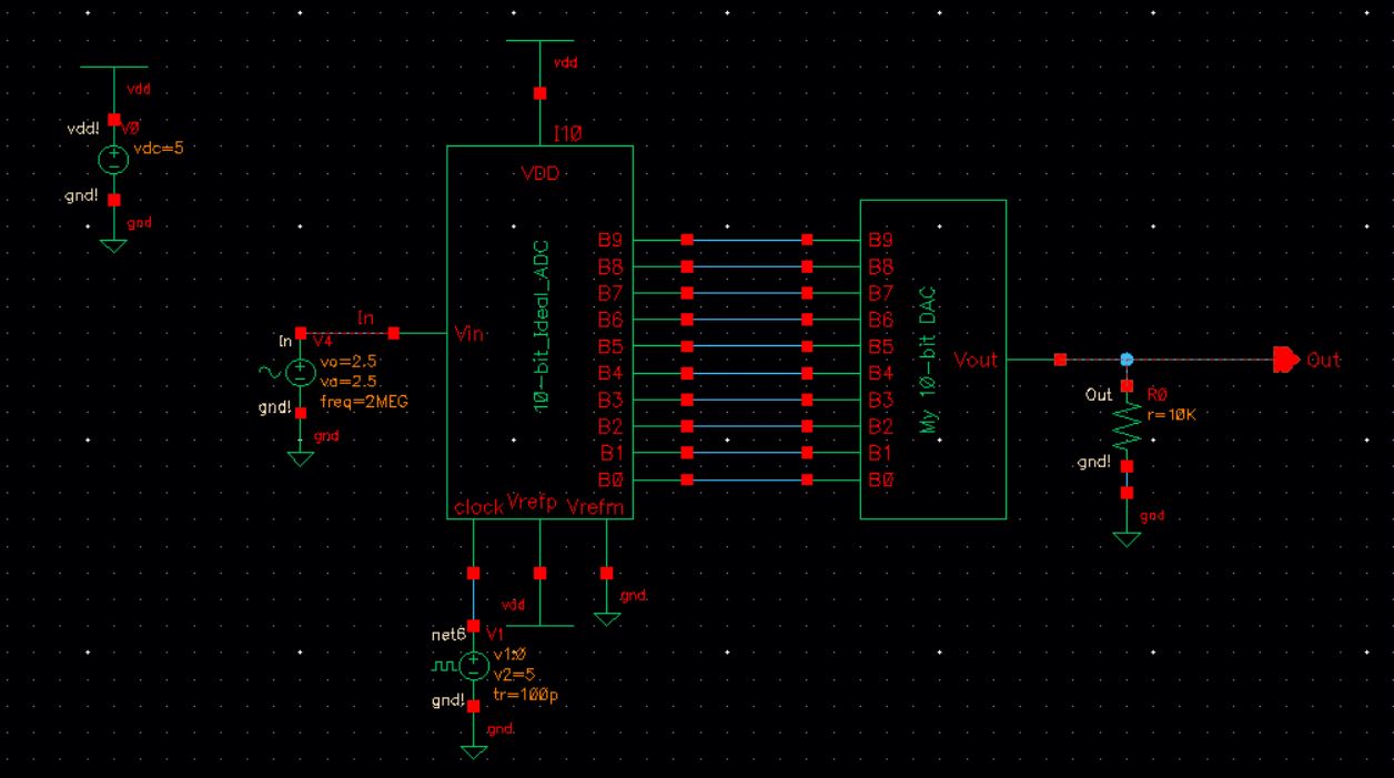
DAC with a 10pF load:
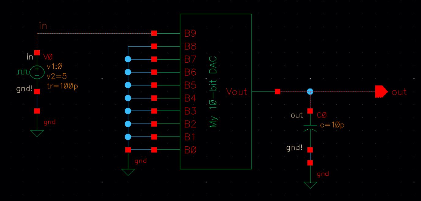
Using the 10-bit DAC created, ground every input except B9 and B9 recieves a 0 to 5V pulse source, after that putting a 10pF capacitor on the output. Before simulating the circuit, predict the time delay.
td = 0.7RC = (0.7)(10K)(10p)= 70ns
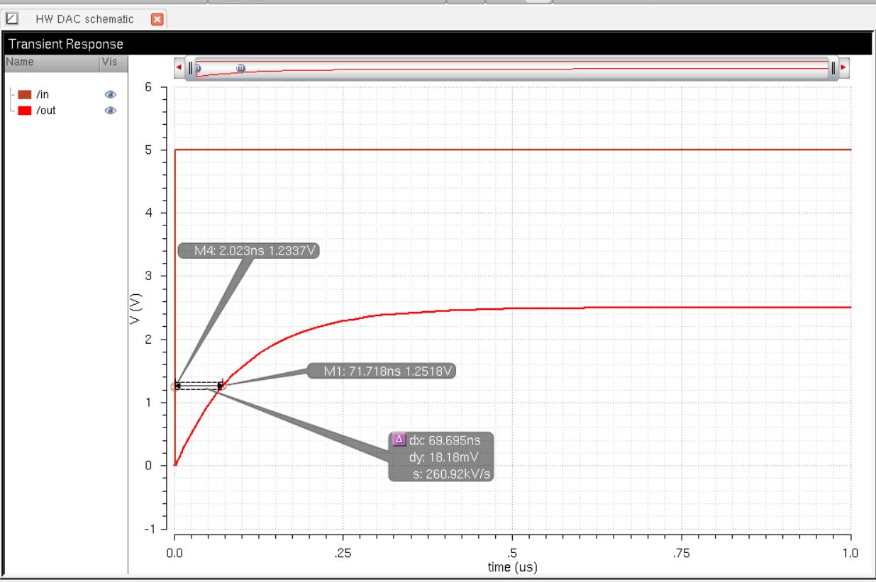
By using the bind key 'm' to mark around half of the input (approximately 1.25V) and using the bind key 'd' adjusting the two marks to make sure they line up, the simulation about shows that the delay equals 69.695ns which is really close to 70ns.
Replacing the ideal DAC with the DAC that was created and simulating it, the similation came out almost looking like the ideal DAC but with the output looking slightly different, this means it works properly.
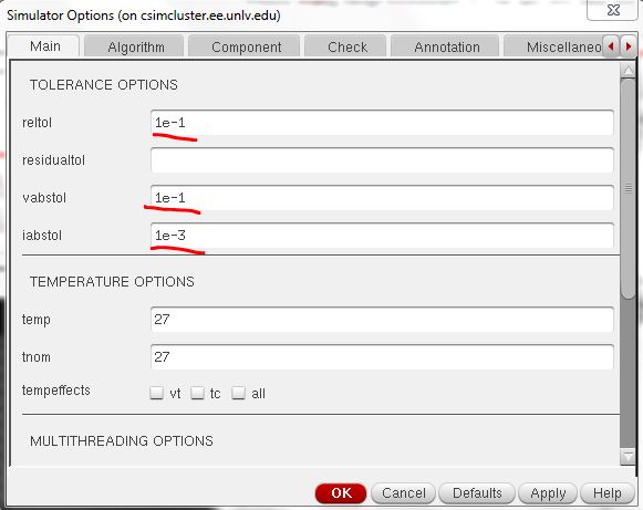
Note: With the current setting on Cadence the similation doesn't finish to 1ns, so to get around this we had to put in the settings shown below.
DAC under 10K resistor load:
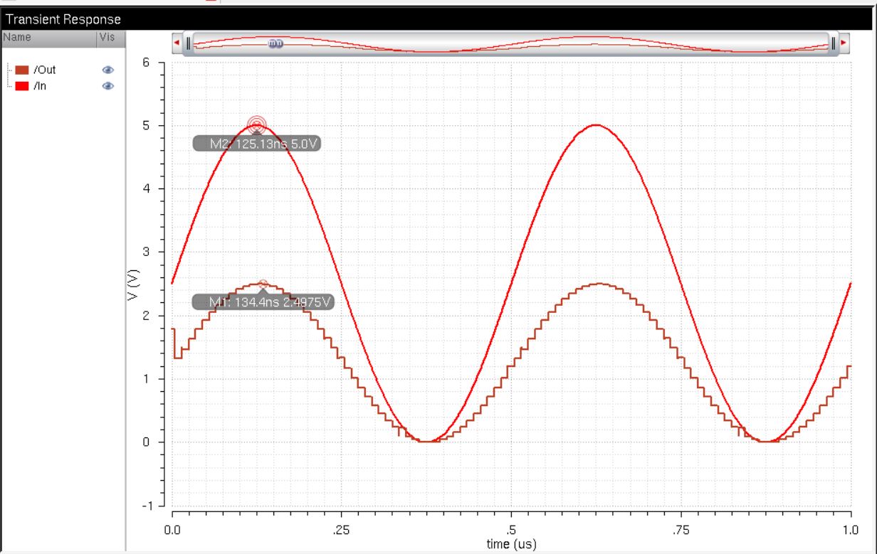
Under the load of the 10K resistor the output is a voltage divider of 1/2 from the input being 5V and output being 2.5V.
DAC under 10pF capacitor load:
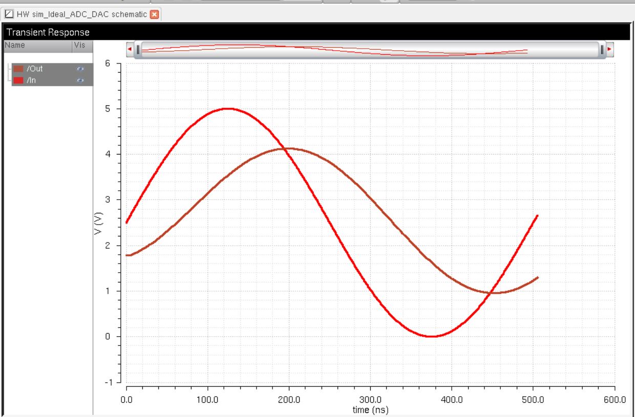
Under a capacitive load the sinusoid is smooth out, but it causes the output the lag the input.
DAC under capacitive and resistive load:
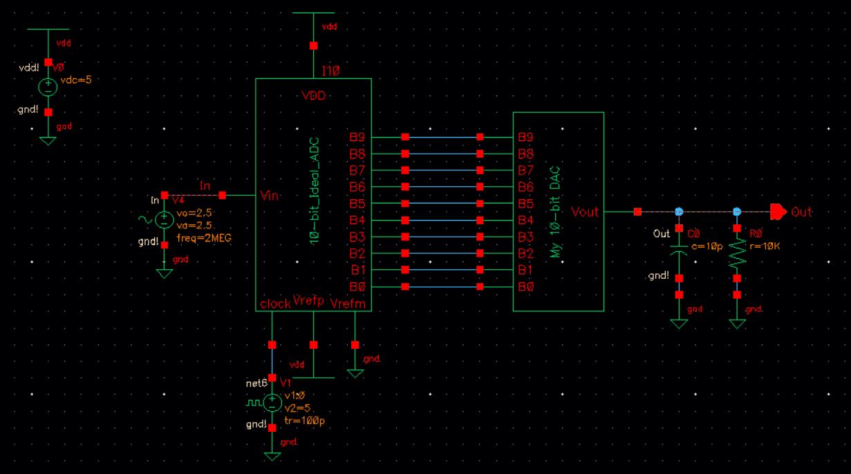
Under both load the output is still halved due to the resistive load being a voltage divider and the wave is smooth out with lag due to the resisitive load.
Back up work by putting it into google drive.