Lab 2 - ECE 421L
Authored
by Quinton Micheau
9/1/2020
micheauq@unlv.nevada.edu
Lab 2
Lab
description
In
Lab 2, we will discuss the functionality behind the DAC. The simulation
was downloaded from the website and unzipped in to the archive using
the instructions provided.
Images:
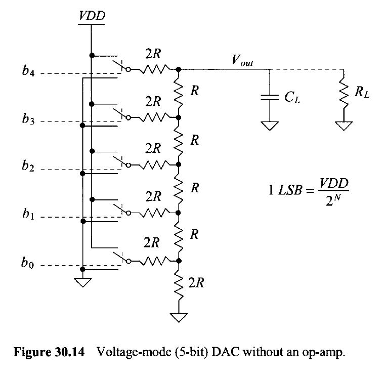
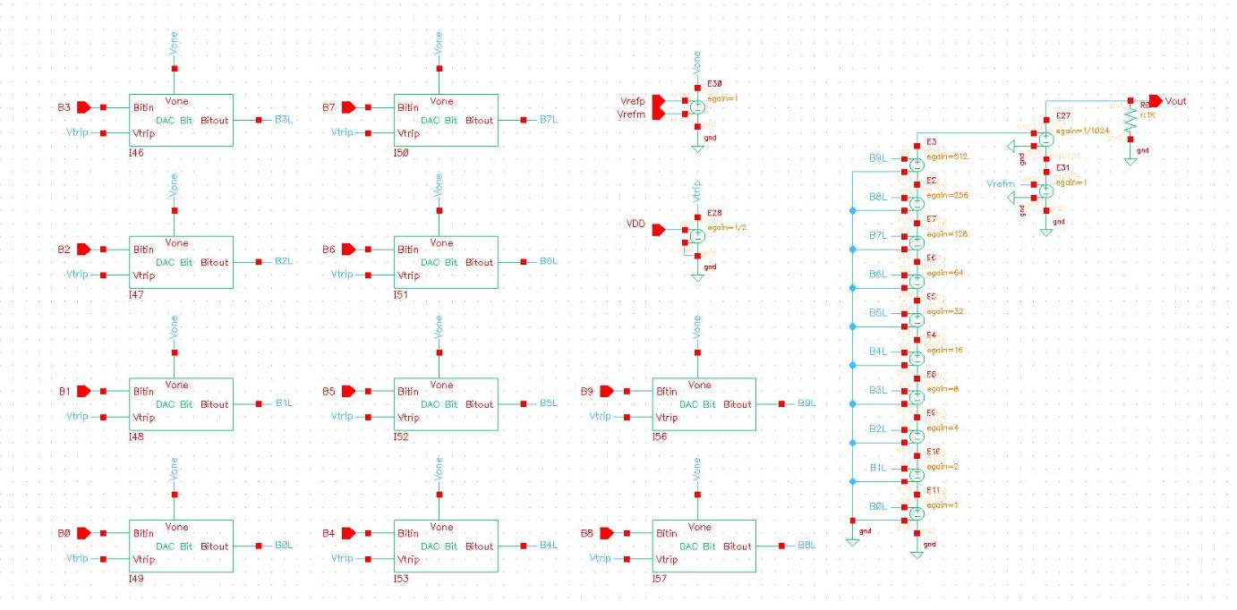
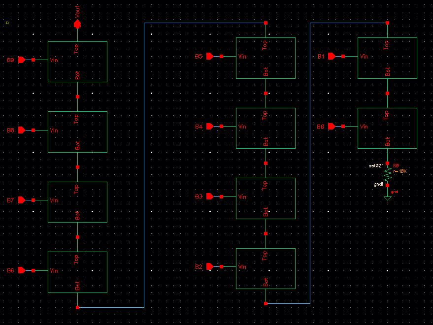
Design of 10-bit DAC
The
design of the 10-bit DAC started with deleting most of the already
provided schematic and replacing each of the individual squares with
the following voltage divider symbol.
Original Design:
Voltage Dividing Schematic:
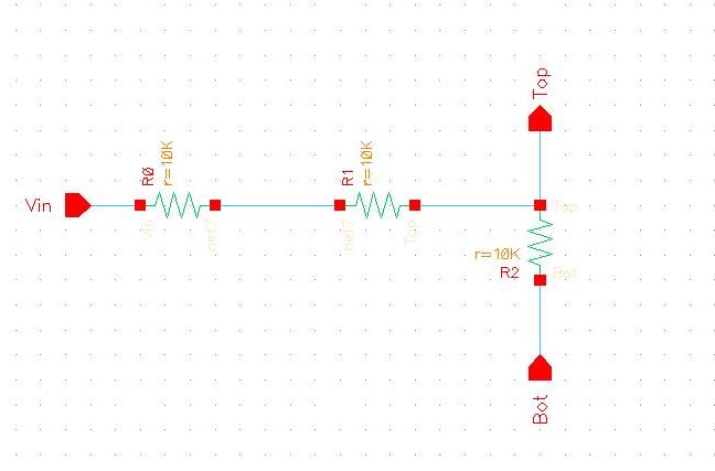
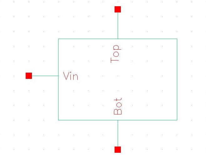
Voltage Dividing Symbol:
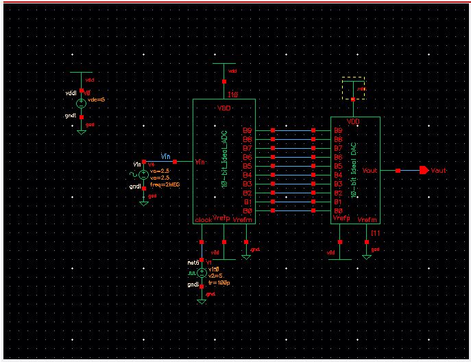
New DAC design :
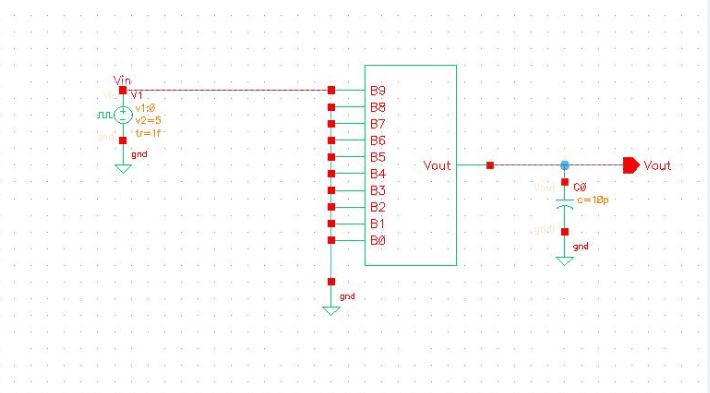
Whole Schematic to be run and tested:
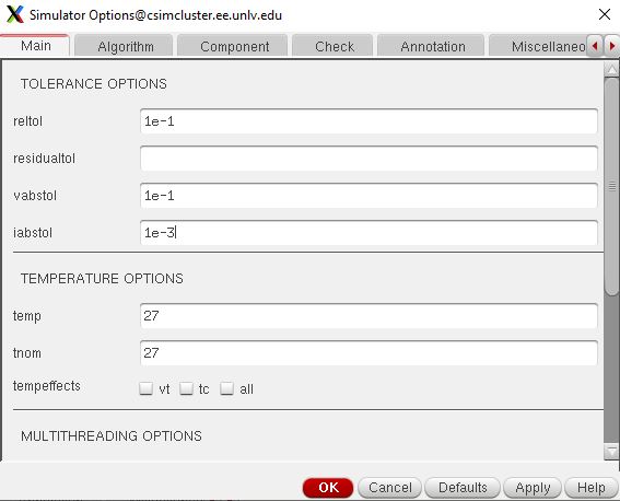
Discussion of Tolerances in Cadence
Before we simulate the above schematic, we need to change the tolerance options in order to force the simulation.
Force the simulation by doing the following:
- ADE, Simulation -> Options -> Analog
- Set the values as seen below
- relative tolerance, reltol, of 10% (= 1e-1)
- voltage absolute tolerance, vabstol, of 100 mV (= 1e-1)
- current absolute tolerance, iabstol, of 1 mA (= 1e-3)
- The accuracy of the simulation will, obviously, be degraded
Results from the Simulation
Driving DAC with a Pulse. 0V -> 5V
Simulation:
Driving DAC with a Pulse. 0V -> 5V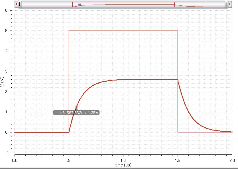
Td From the image:
567ns - 500ns = 67ns
Td from Calculations:
(0.7)RC = (0.7)(10E3)(10E-12) = 7E-8 = 70 ns
Therefore, the simulation holds true to the calculations.
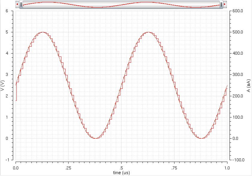
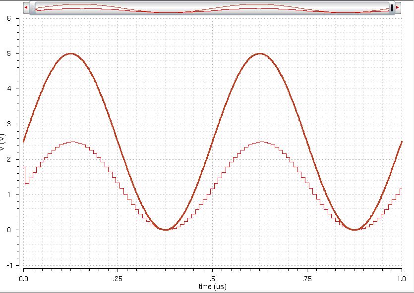
Driving DAC an Ideal ADC with no load:
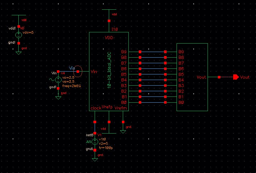
Results:
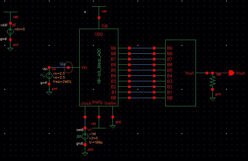
Driving DAC an Ideal ADC with a 10k load:
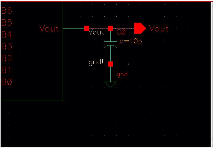
Driving DAC an Ideal ADC with a 10pF load:
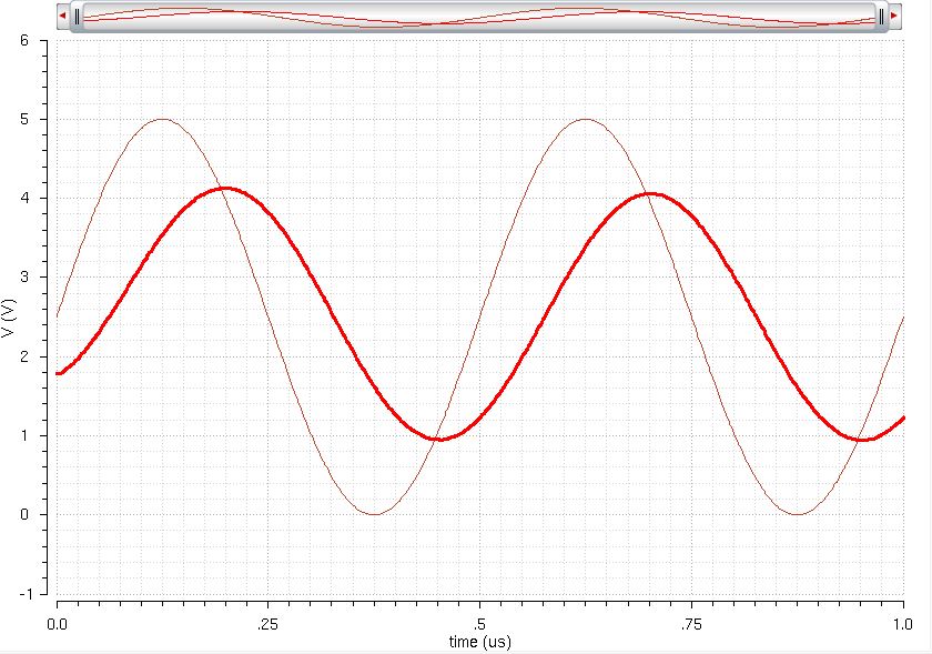
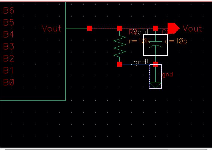
Driving DAC an Ideal ADC with a 10k and 10pF in parallel load:
Return to EE 421L Labs