Lab 6 - EE 421L Fall 2020
Authored by Abraham Lopez on 10/19/20
Email: lopeza43@unlv.nevada.edu
Lab description
The purpose of this lab was to create schematics, symbols, and layouts first, for a NAND gate, then for an XOR gate.
Then, taking those symbols and layouts to make a full adder, and making sure the layout DRC and LVS.
Pre-lab
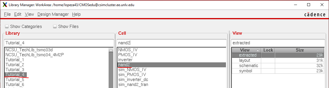
For the pre-lab we saved and backed up our previous work, read through the lab guide, and did tutorial 4.
The first part of the tutorial involved creating a NAND gate circuit, but before that we created a tutorial 4
library by coping tutorial 3 and renaming, then making a nand cell schematic.
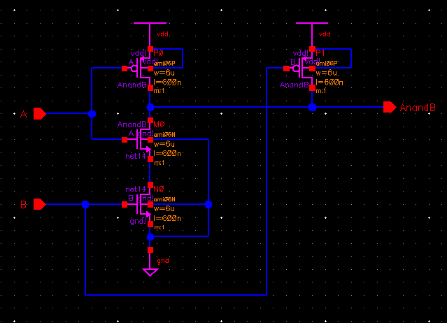
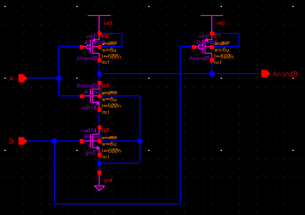
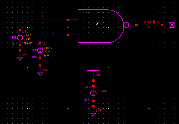
Then we create the following circuit for the NAND gate seen below.
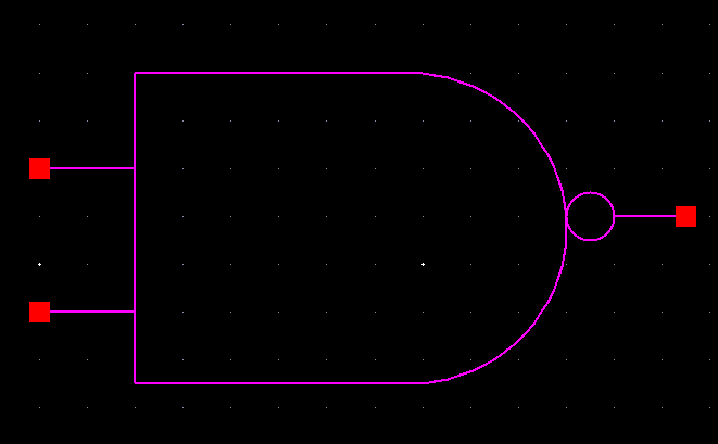
From that schematic we want to create a symbol for it.
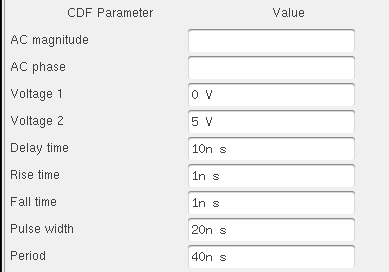
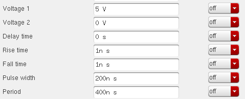
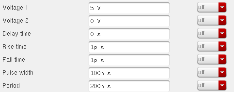
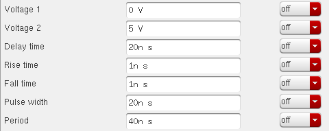
With those steps complete, we'll create a simulation schematic with the following parameters for the voltage pulse.
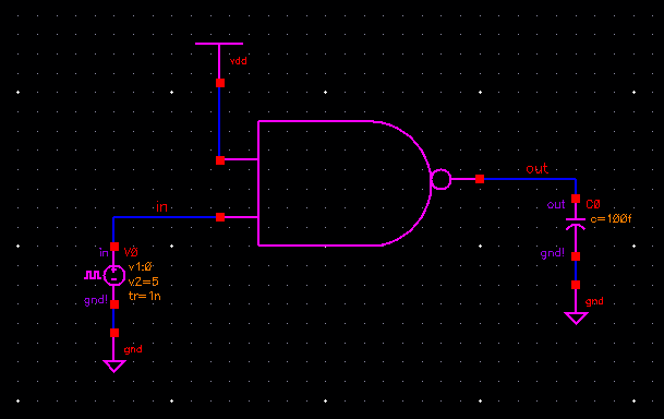
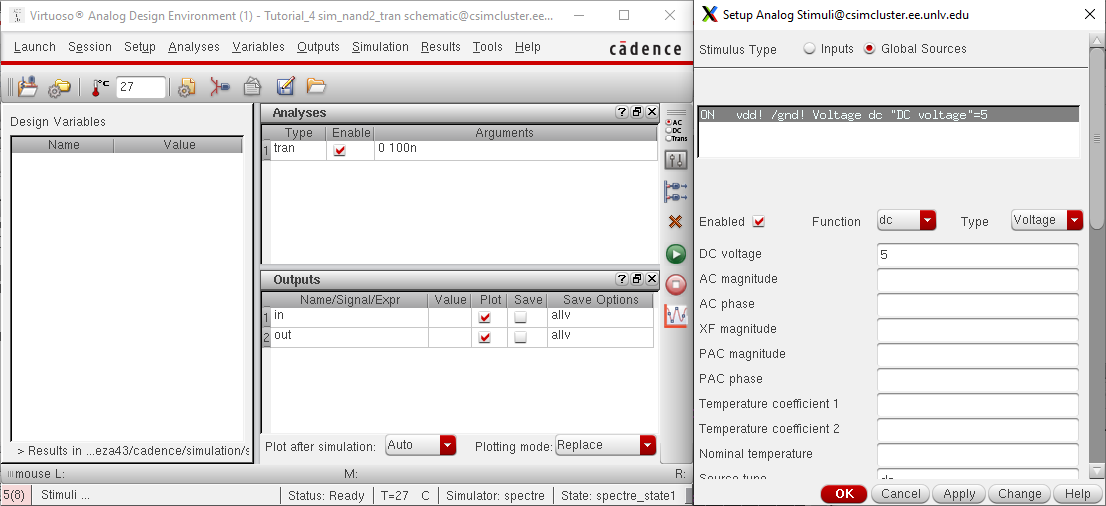
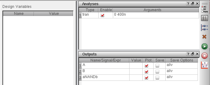
Then launching the ADE simulator and setting it up with the following options. Also setting up a stimuli for the vdd.
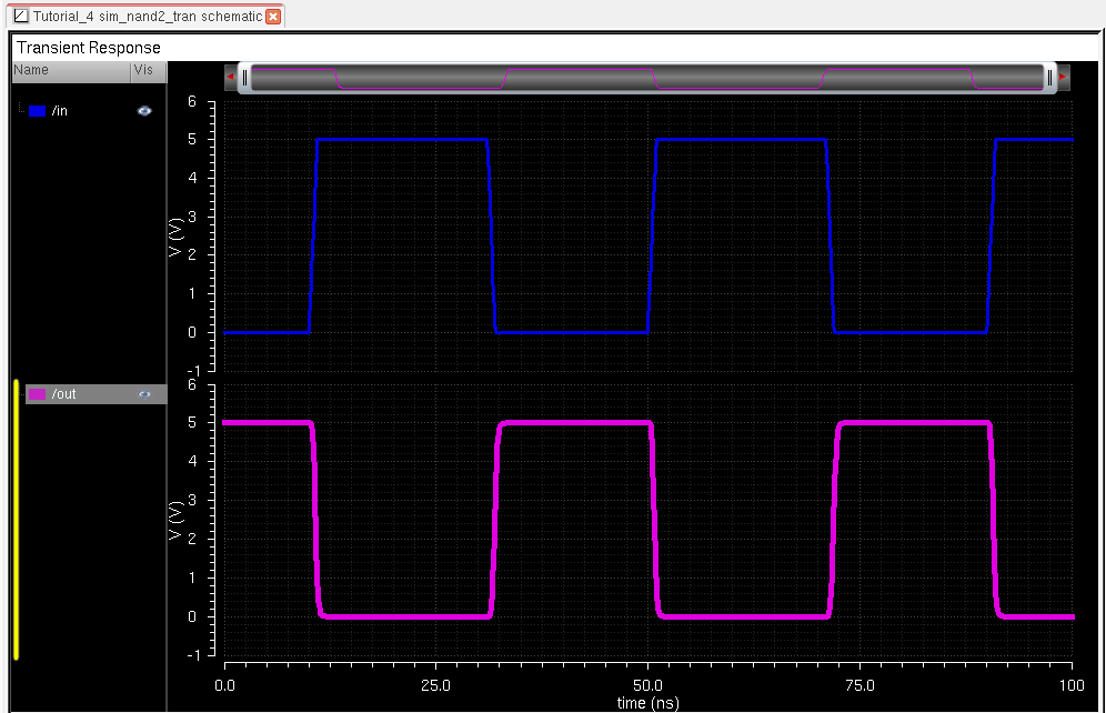
Simulation of the NAND gate, where vdd is always "1" and in switches between "0" and "1". Giving the output where
"0" and "1" give an output of "1" , otherwise a "1" and "1" give an output of "0".
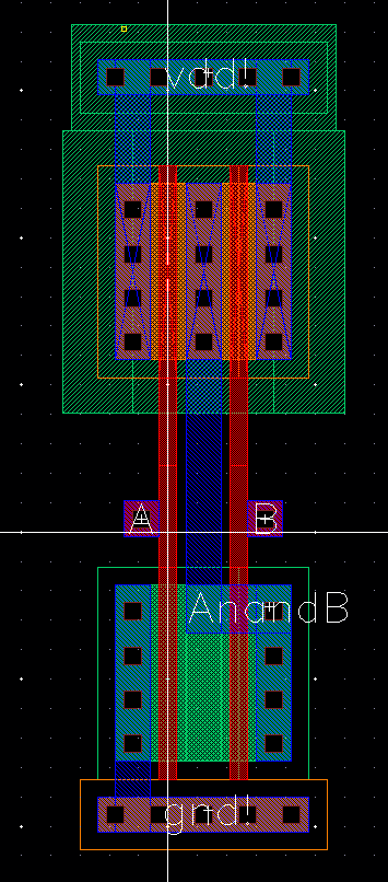
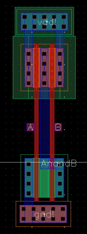
We than create a layout of the NAND gate, and notice for the bottom NMOS, the middle terminal is gone,
as used the "flatten" option on the NMOS to edit the layers and remove the terminal we weren't going to use.
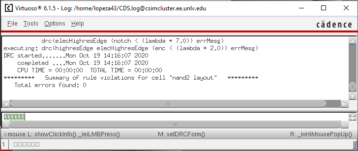
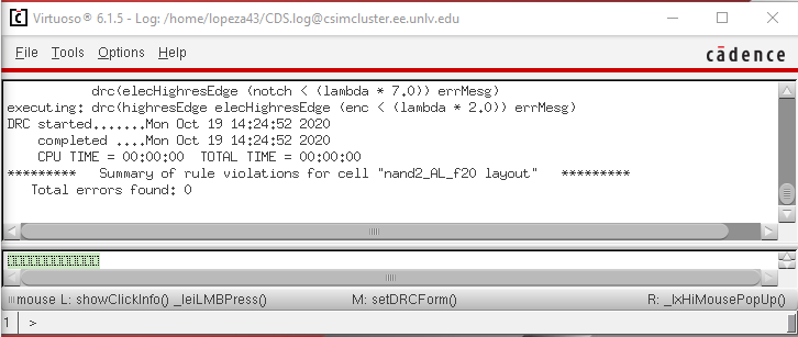
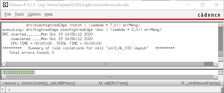
DRC of layout.
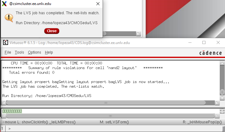
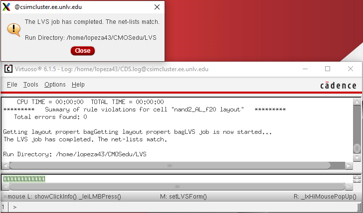
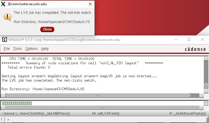
LVS of layout.
This ends the pre-lab.
Lab Procedures
1. Drafting and testing a 2-input NAND gate.
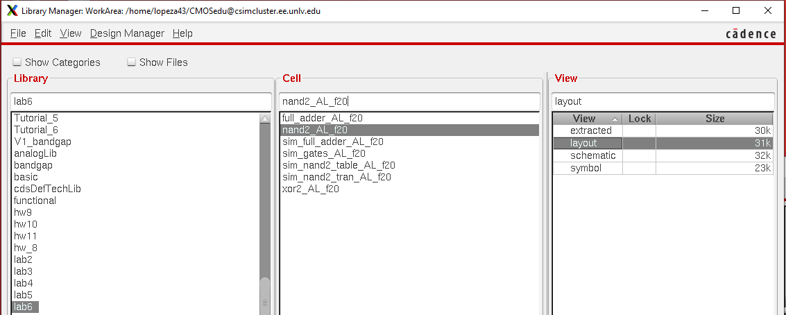
First create a new library called "lab6" and then make a cell view for the nand schematic.
Drafting the schematic for the NAND gate.
Creating a symbol for it, and also making sure to add a text box to it of my initials.
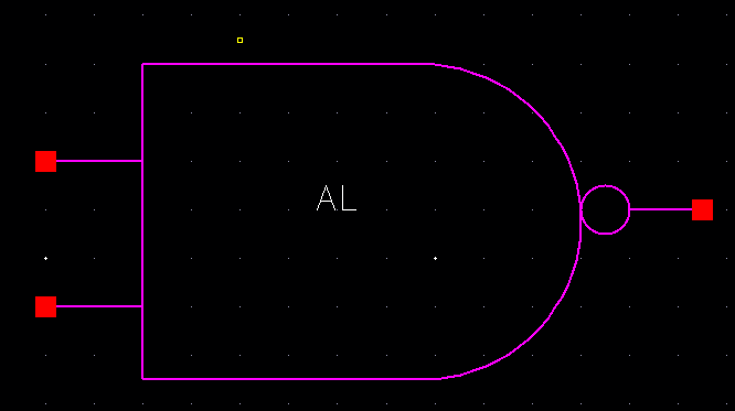
Layout of the NAND gate, which is the same from the pre-lab.
DRC and LVS of the layout.
Now testing the schematic and layout by making a simulation schematic and state.
Also we need different parameters for each voltage pulse.
Settings of the ADE and results of the simulation.
2. Drafting and testing a 2-input XOR gate
First we create a new cell view for the xor schematic and draft the schematic.
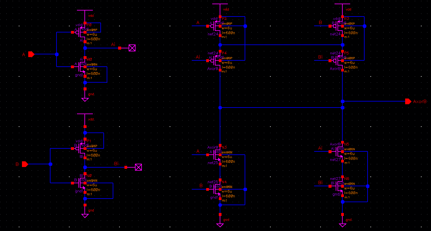
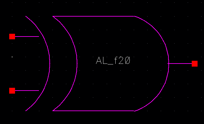
Making a symbol for the schematic with the same method used for the NAND gate.
Layout of the XOR gate.
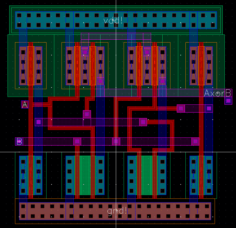
DRC and LVS of the layout.
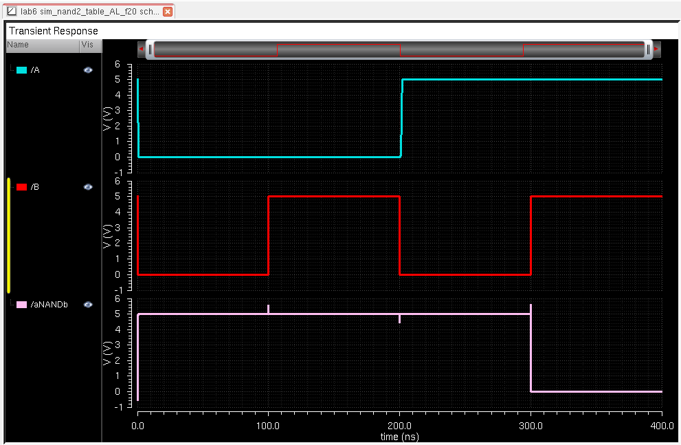
Now we will simulate our XOR gate along with the NAND gate and inverter.
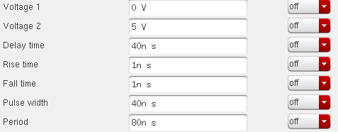
Parameters for the voltage pulses.
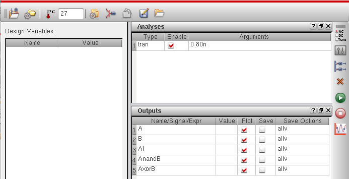
Settings for the ADE and simulation results.
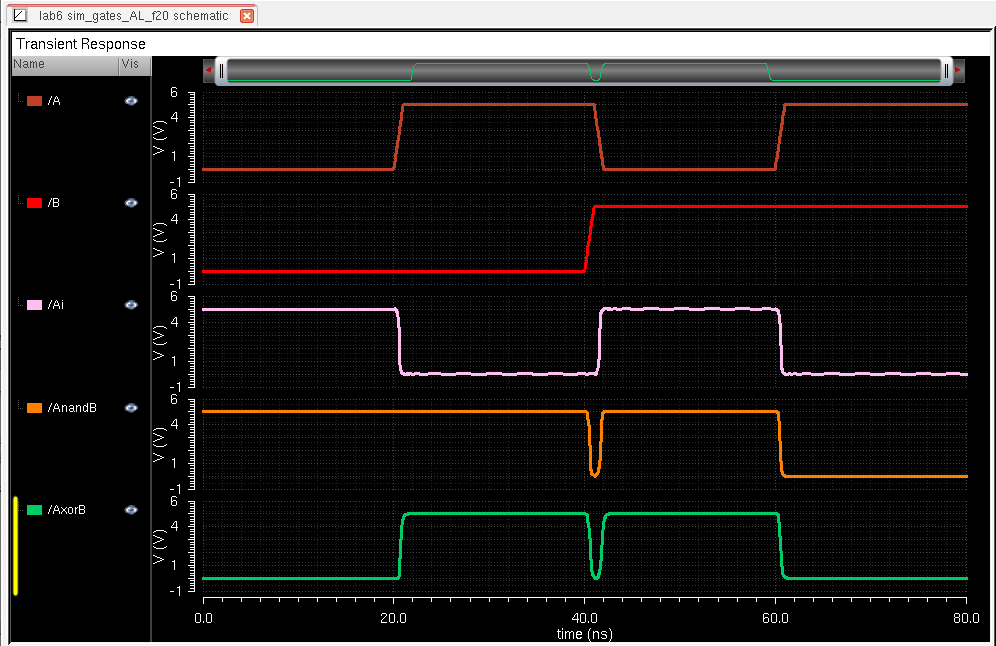
Notice that with these simulations there always seem to be these glitches. These glitches occur from the
input pulses, specifically the rise and fall times where the inputs switch from high to low or vice versa. The moment
that these occur the output reflects these changes from the input for however long the rise/fall time is.
3. Drafting and testing a full adder.
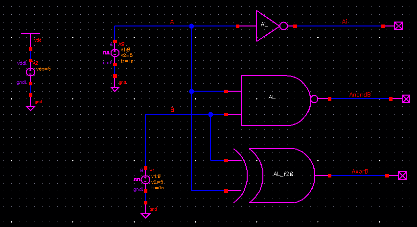
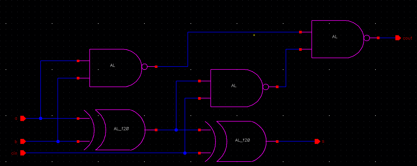
Creating a new cell view for the full adder, and drafting the schematic seen below using the
symbols we've been making through the lab.
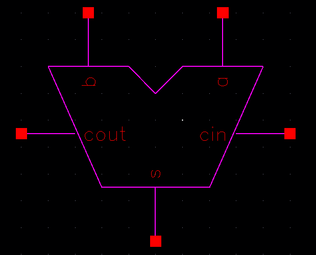
Creating a symbol for the schematic.
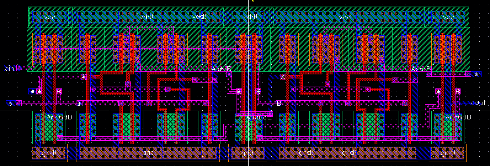
Layout of the full adder.
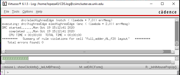
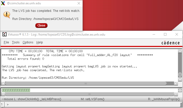
DRC and LVS of the layout.
We are now going to simulate the full adder with the simulation schematic seen below.
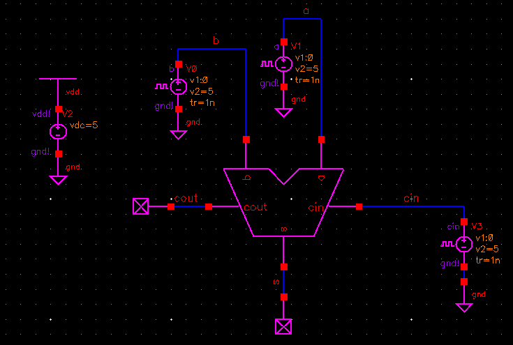
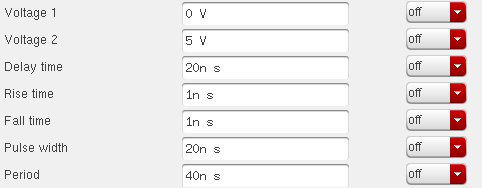
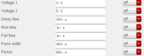
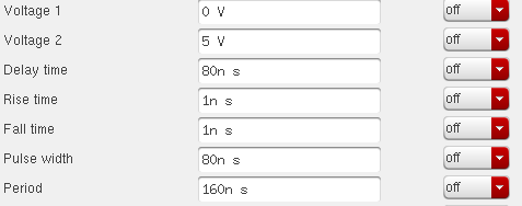
Parameters for the voltage pulses.
Results of the full adder simulation.
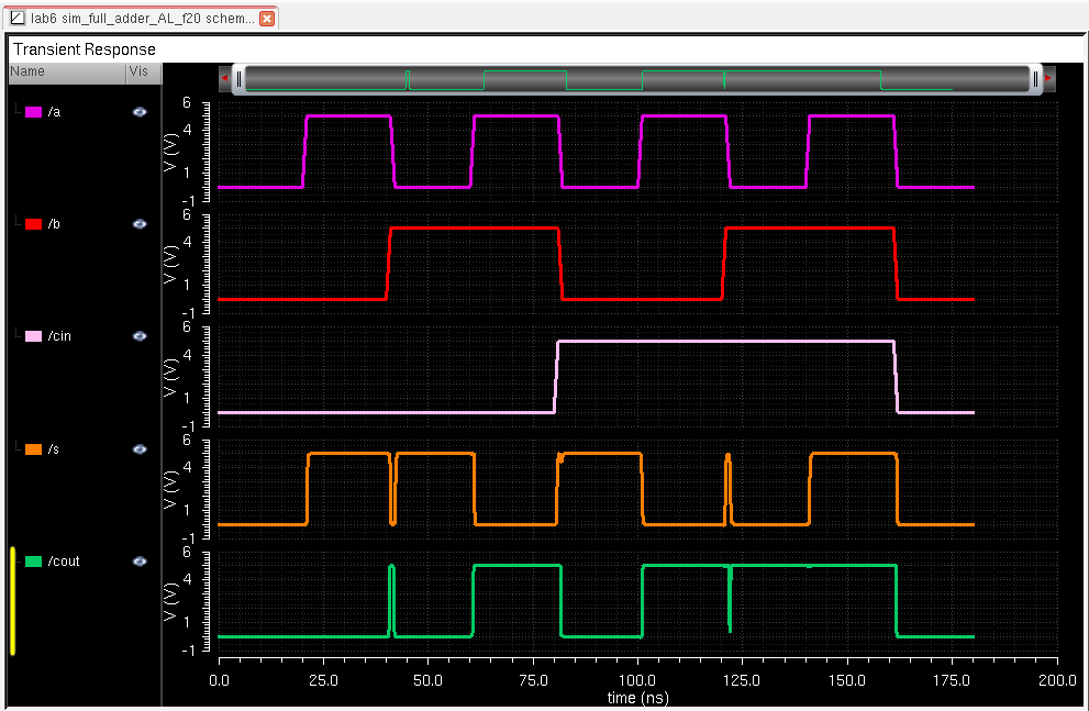
Again notice that the glitches are happening due to the change of inputs during the rise
and fall times. Even adding inverters to try and deal with this won't resolve the issue entirely,
but it will help.
4. Backing up work
I downloaded and zipped up the lab 6 folder.
Then emailed myself a copy.
This concludes the lab.
Go Back to Laboratory reports