Lab 4 - EE 421L Fall 2020
Authored by Abraham Lopez on 09/16/20
Email: lopeza43@unlv.nevada.edu
Lab description
The
purpose of this lab is to simulate NMOS and PMOS devices through
simulations with different parameters. Also create layouts of
these devices and insure they pass DRC and LVS, then simulate the extracted layouts.
Pre-lab
For this pre-lab we had to back up our previous work, read through the lab guide, and go through Tutorial 2.
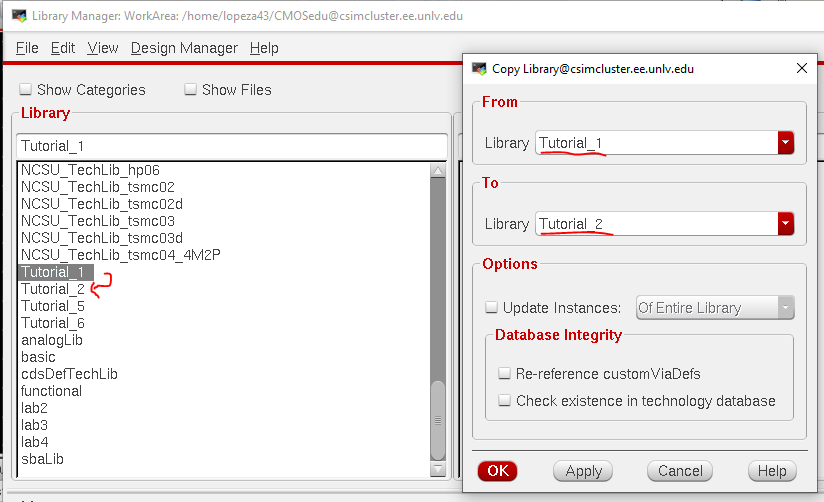
First we will create a new library by copying tutorial 1 and renaming it tutorial 2
Then we will create a new cell schematic and make the following schematic seen below
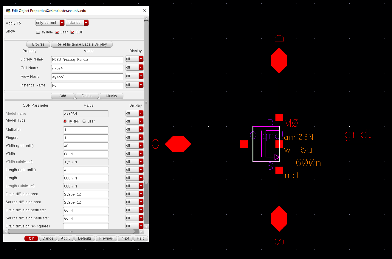
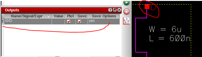
This schematic is composed of an 4-channel nmos transistor, where the width and length
of the channel are changed to 6 um and 600 nm via the properties menu.
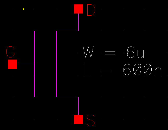
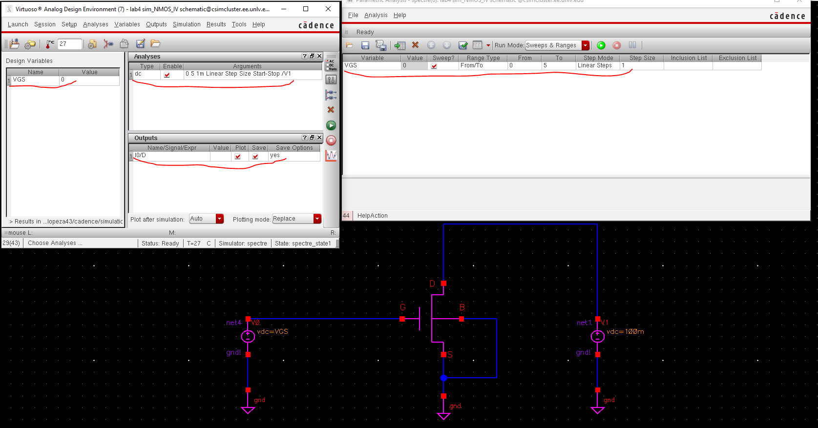
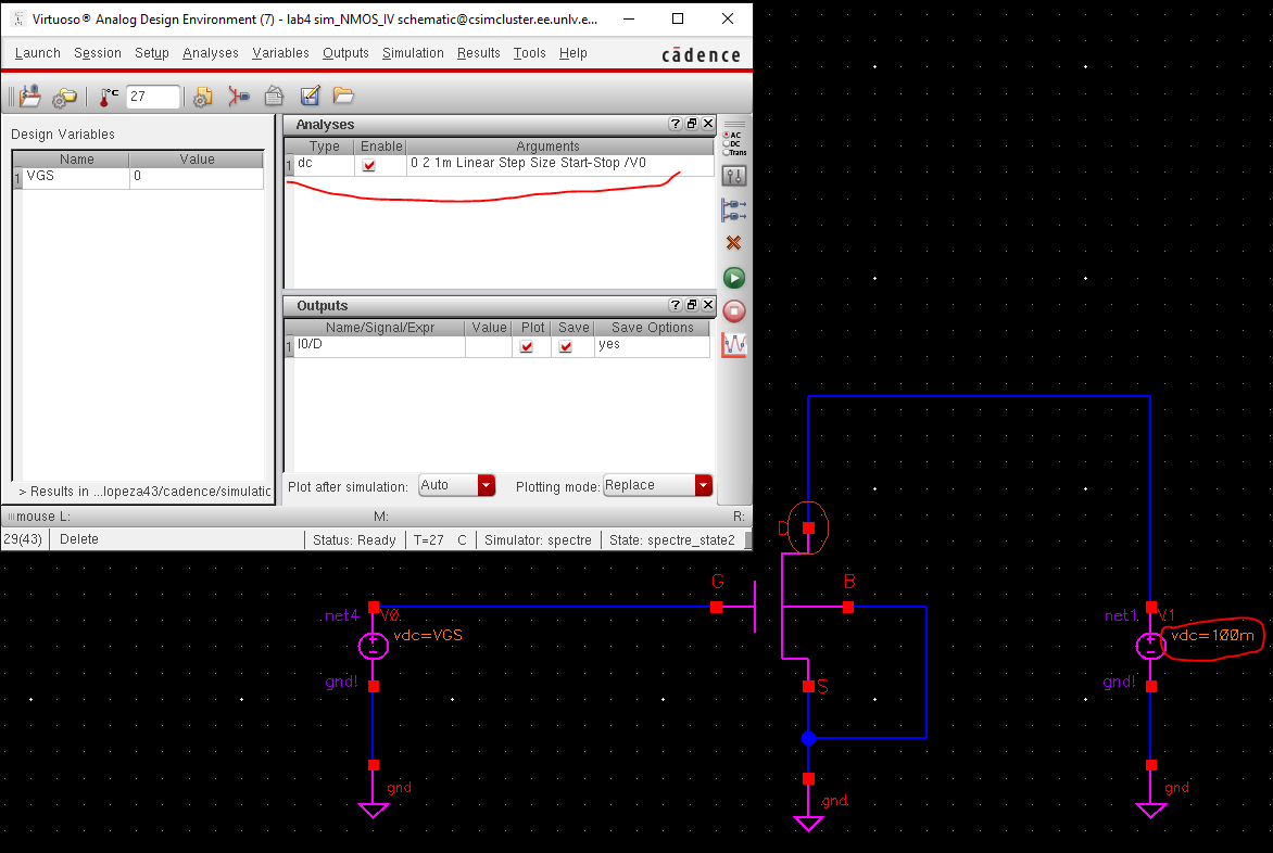
We then want to create a symbol for this schematic and make another schematic cell that will simulate the nmos.
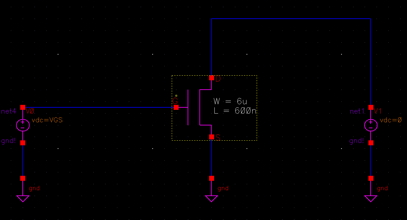
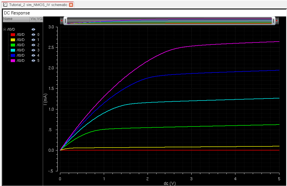
For this simulation we want to have V0 to be vdc = VGS and V1 to be vdc = 0.
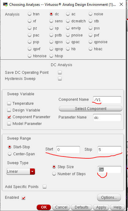
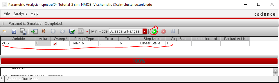
We
then want to create a simulation state based on the parameters seen
below, where V1 is dc sweep from 0 V to 5 V with a linear step of 1 mV.
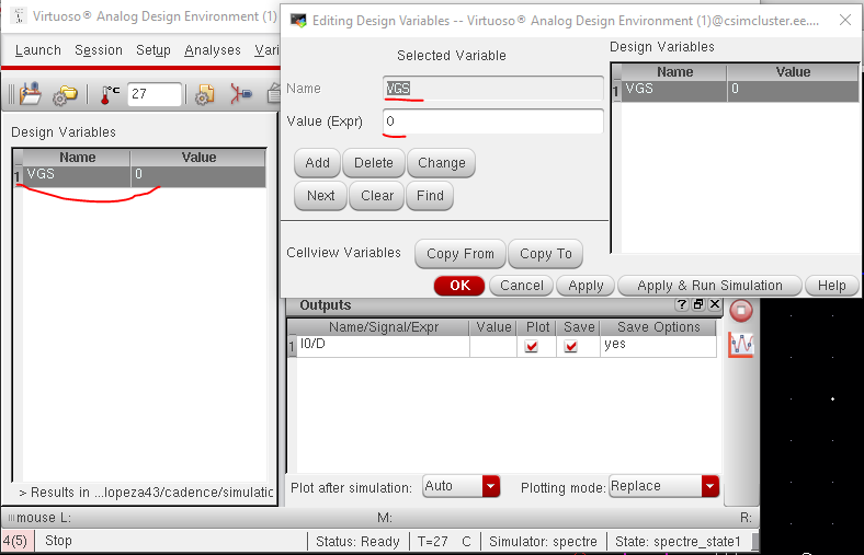
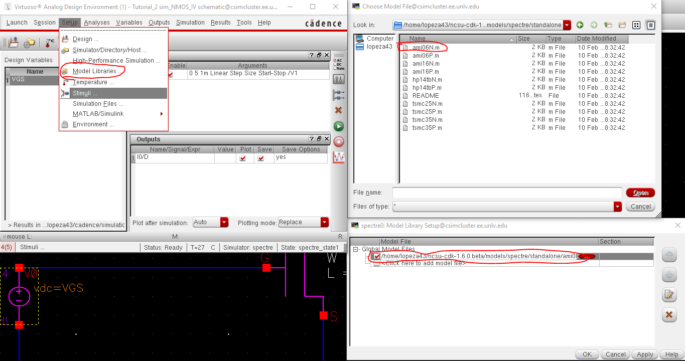
We
also want to add a design variable VGS and set it equal to 0, then go
to the "Setup" menu and click on "model libraries" and selecting
the ami06N file by following the path directory "ncsu-cdk-1.6.0.beta/models/spectre/standalone/ami06N.m".
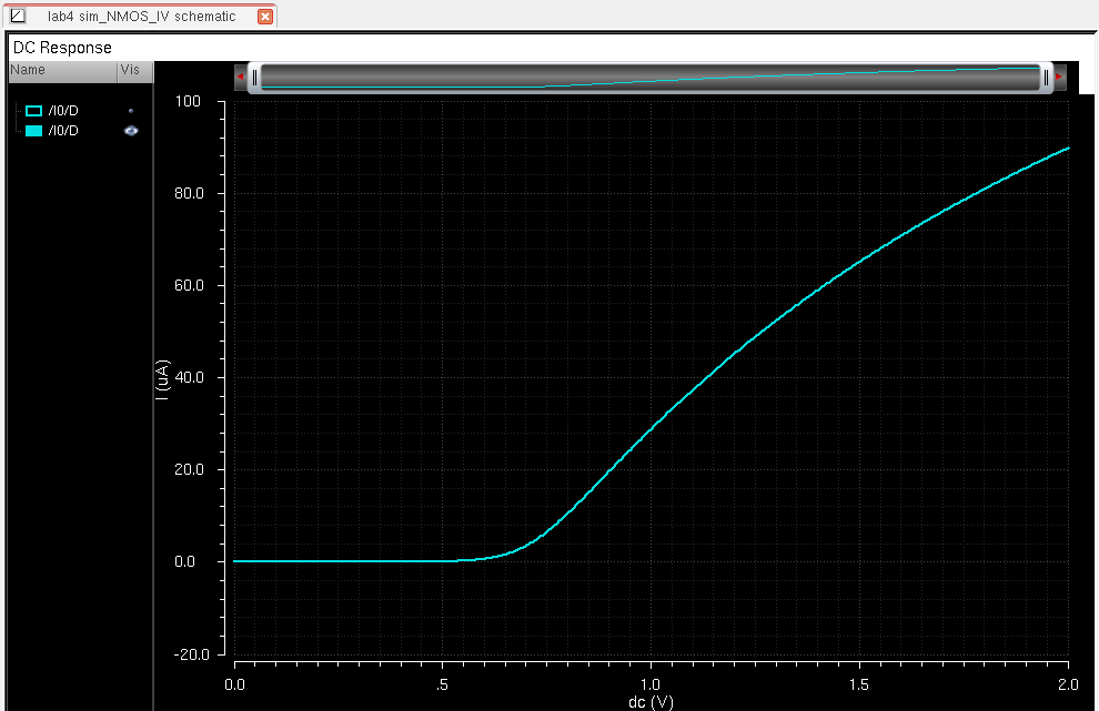
Next we want to plot the current of the drain of the nmos or node D, then we want to go to the "Tools" menu
and click on "parametric analysis" and set a dc sweep from 0 V to 5 V with a linear step of 1 V, and then start
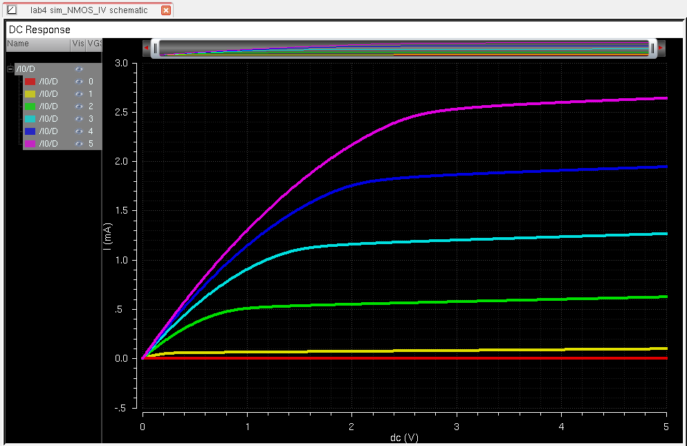
an analysis by clicking the green button and viewing the following waveform.
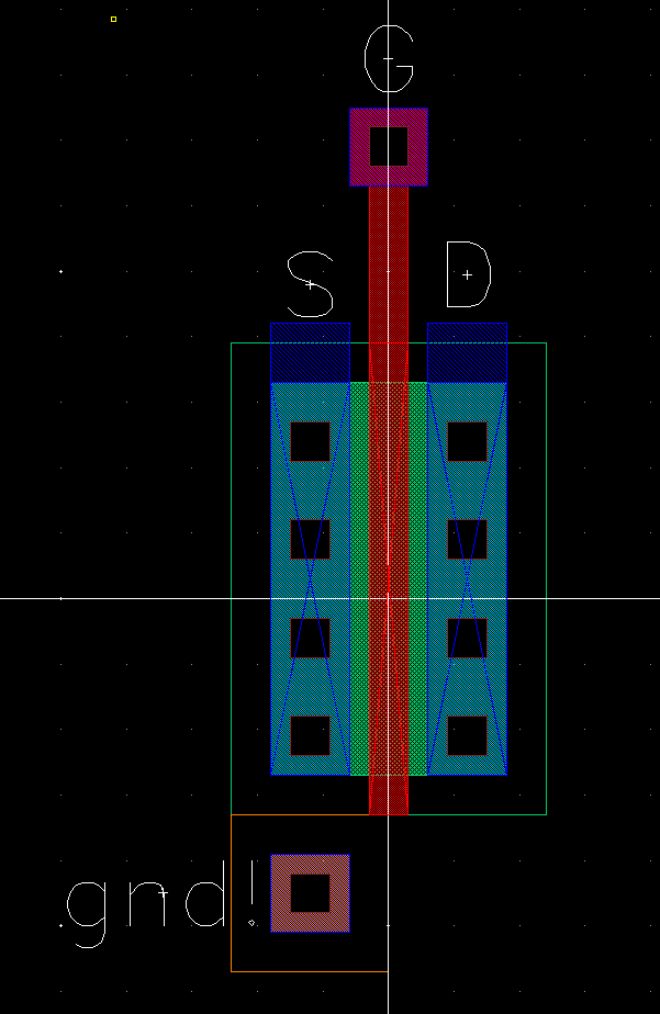
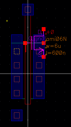
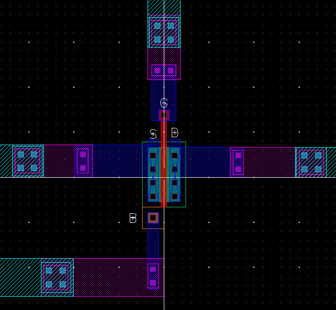
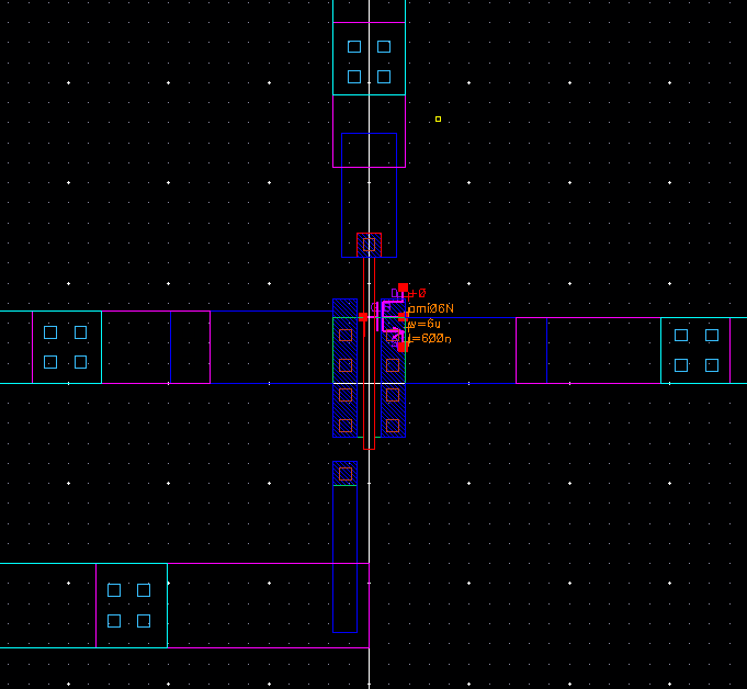
Now we are going to create a layout of the nmos, we accomplish this by instantiating from the ami06 library an nmos layout and
we also want to instantiate a m1_poly layout and a ptap. Then we want to draw a poly layer to the m1_poly layout and place
metal 1 layer pins of gnd! on the ptap, G on the m1_poly, then S and D on the left and right contact cuts.
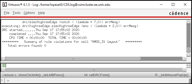
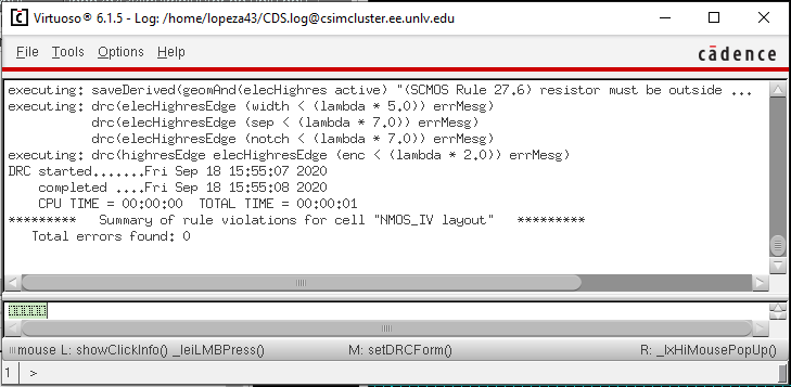
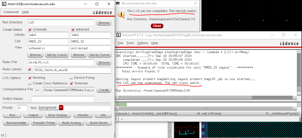
Now we will DRC, extract, and LVS the layout.
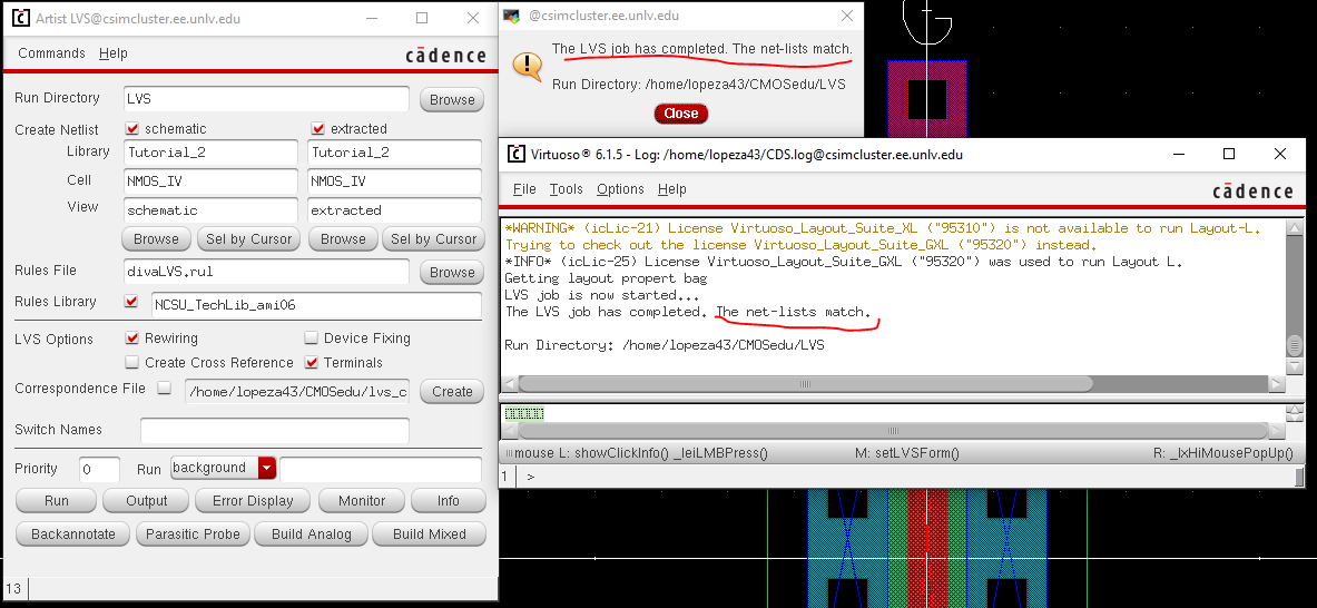
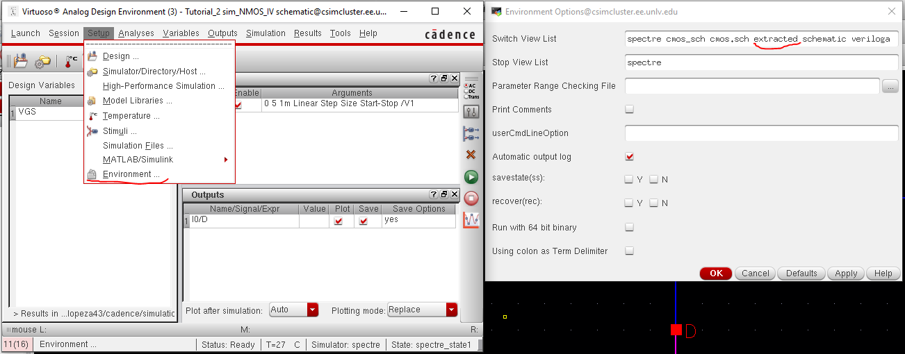
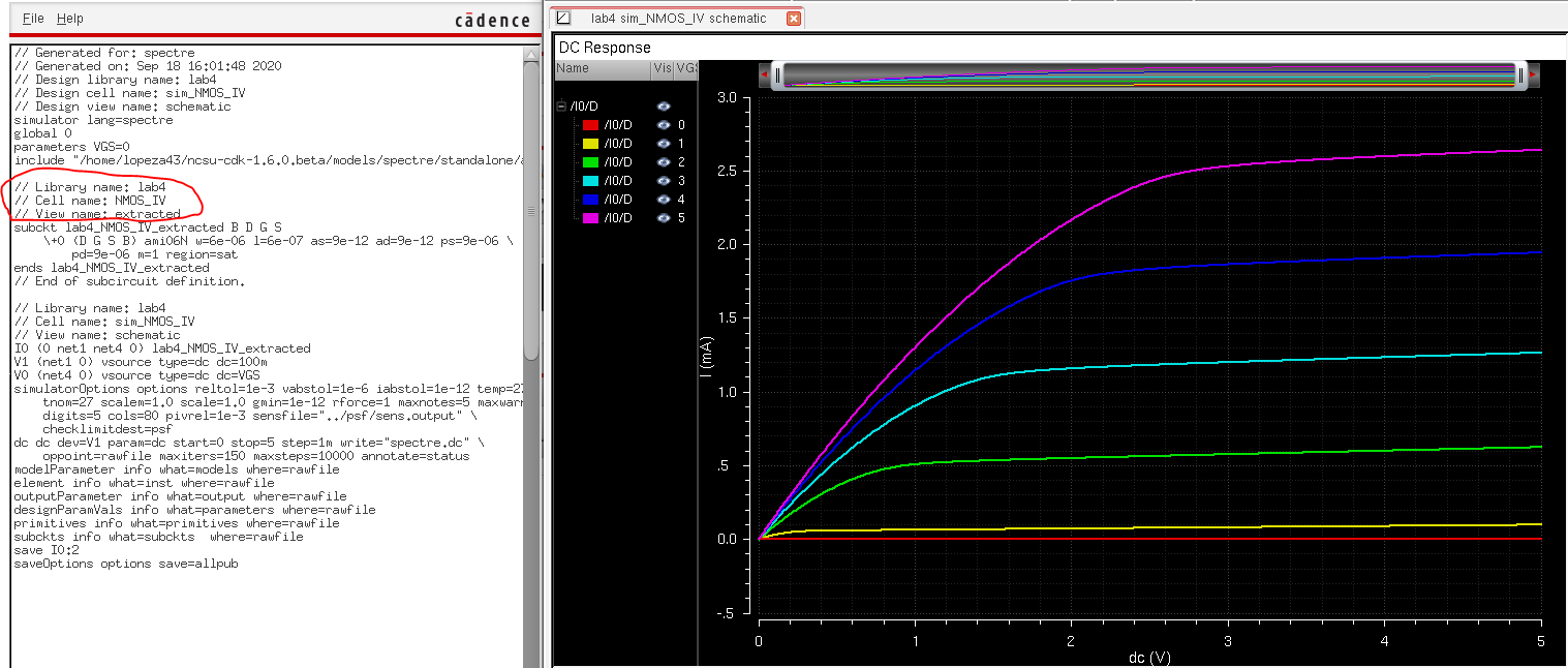
Then we will simulate this extracted layout by opening the simulator and clicking on "Setup" and selecting "Environment", then
typing in the switch view list "extracted" right between cmos.sch and schematic.
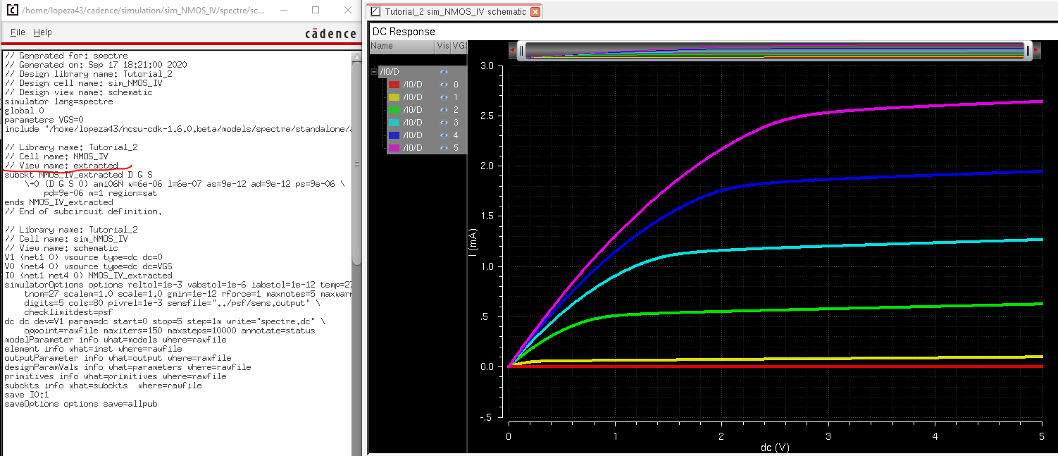
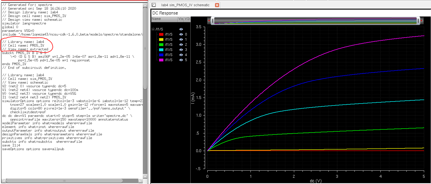
Then using the same steps above when we simulated the schematic, we got the following results for the extracted simulation.
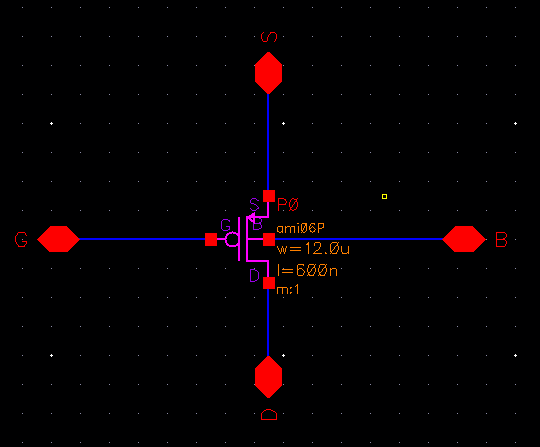
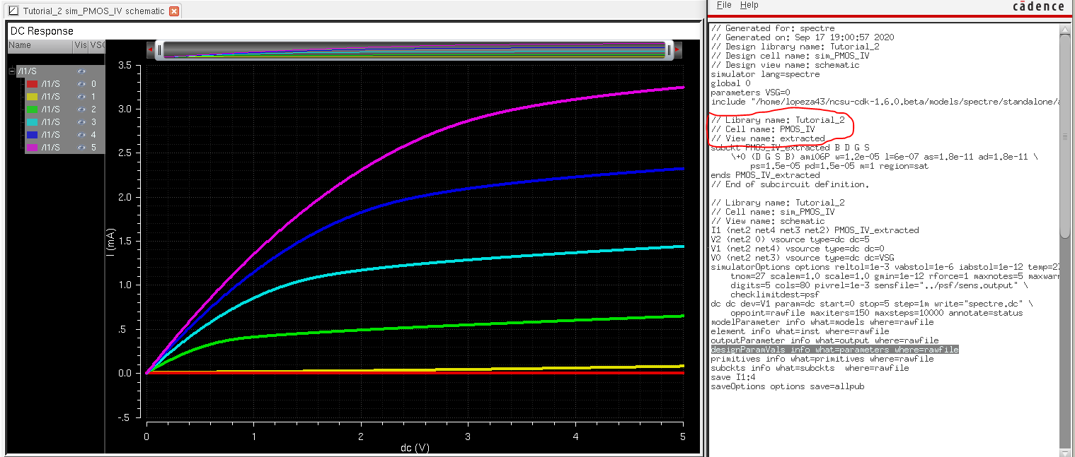
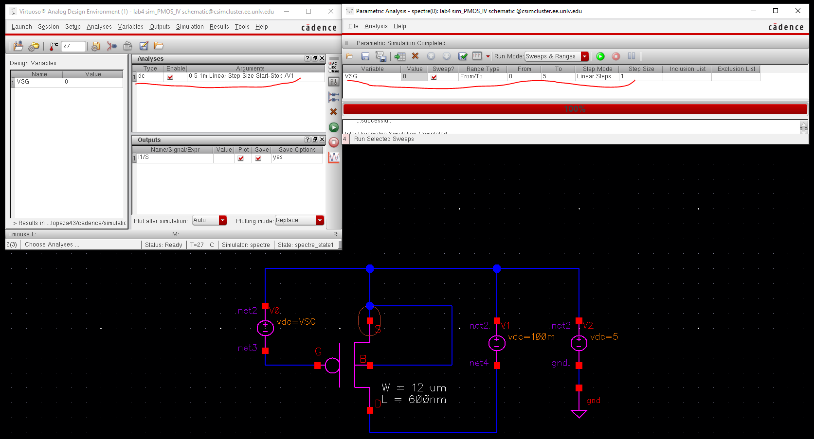
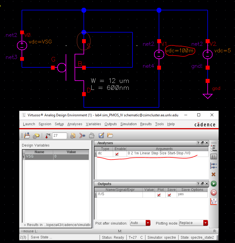
We are now gonna repeat the same steps for the 4-channel pmos transistor, with creating a schematic of it with a
channel length and width of 12 um and 600 nm.
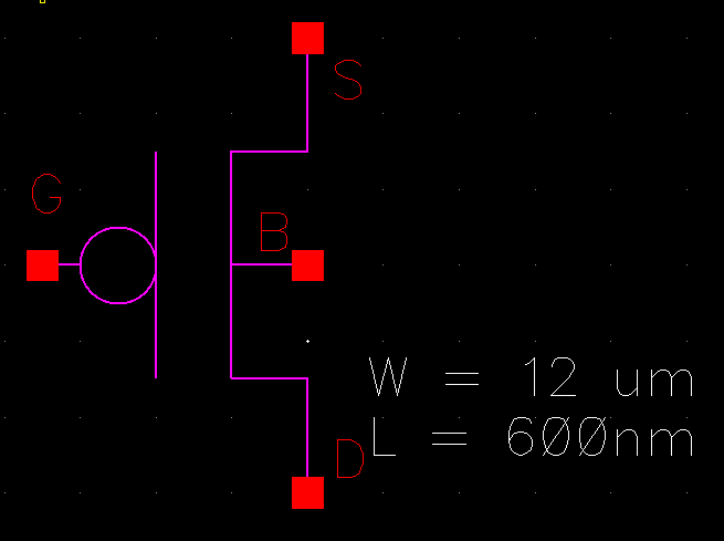
Next we create a symbol from the cell view and simulate the schematic with the same steps we did with the nmos.
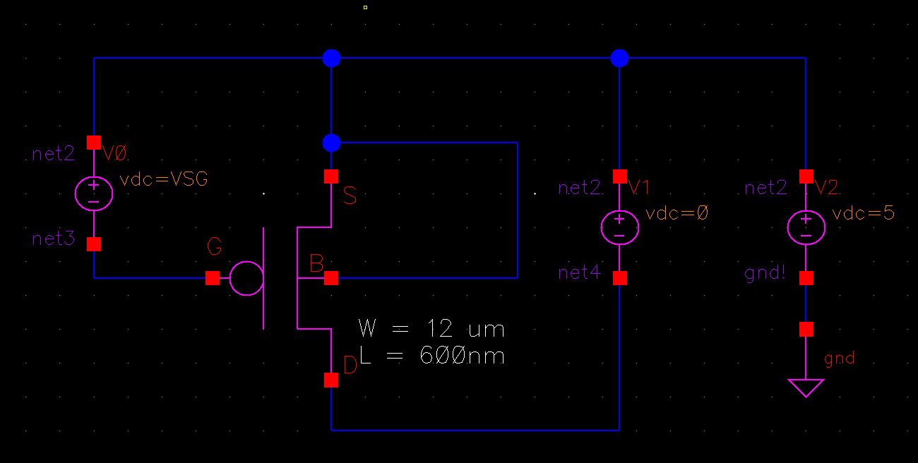

Notice that this schematic is a bit different, with the body tied to the source and V0 is vdc = VSG (Not VGS), V1 is vdc = 0,
and V2 is vdc = 5.
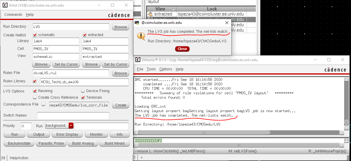
We then create the layout of the pmos , DRC, extract and LVS the design.
Finally we simulate the extracted design.
Lab Procedures
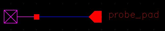
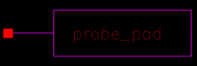
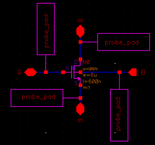
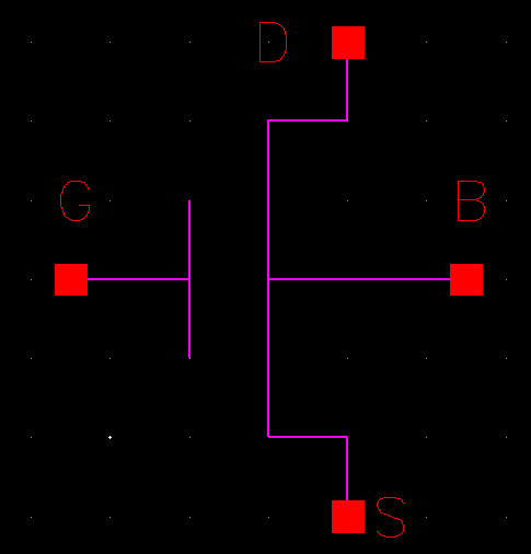
1. Creating a probe pad schematic and layout
For this first part of the lab we create a schematic of a probe pad and also making a symbol for it.
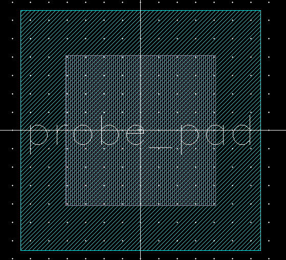
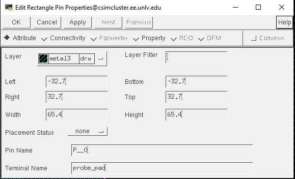
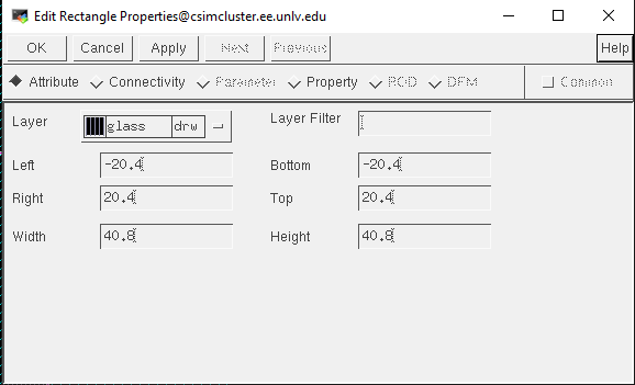
Then we want to create a layout that follows the MOSIS design rules with a metal 3 layer and a glass layer. Where
the metal 3 layer is 32.7 um x 32.7 um and the glass layer 20.4 um x 20.4 um.
2. Simulations of 4-channel NMOS transistor under different parameters
ID v. VDS of an NMOS device for VGS varying from 0 to 5 V in 1 V steps while VDS varies from 0 to 5 V in 1 mV steps.
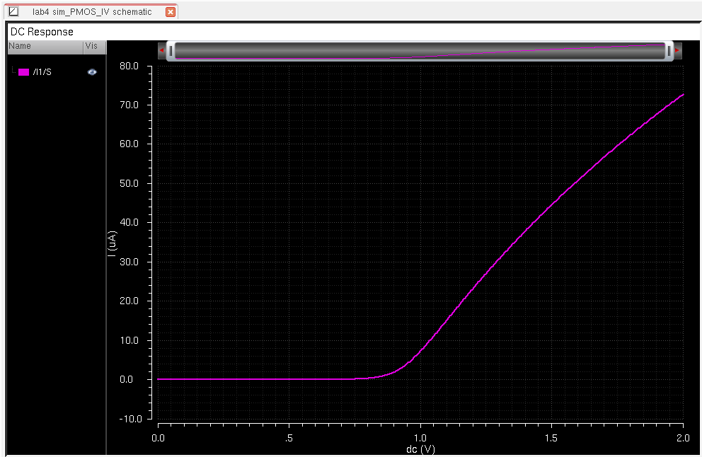
ID v. VDS of an NMOS device for VDS = 100 mV where VGS varies from 0 to 2 V in 1 mV steps.
3. Simulations of 4-channel PMOS transistor under different parameters
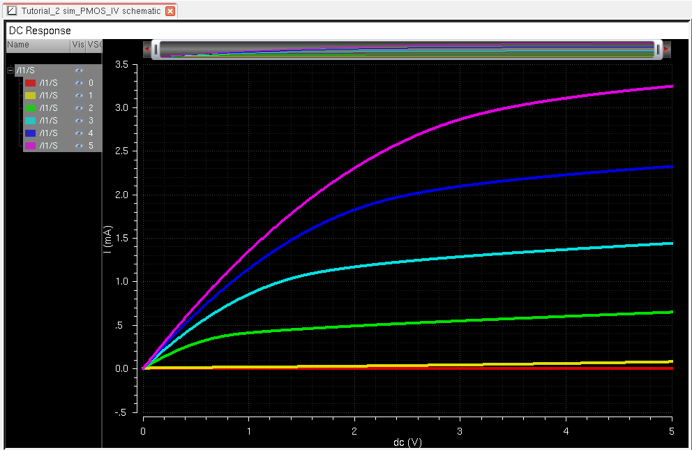
ID v. VSD of an PMOS device for VSG varying from 0 to 5 V in 1 V steps while VSD varies from 0 to 5 V in 1 mV steps.
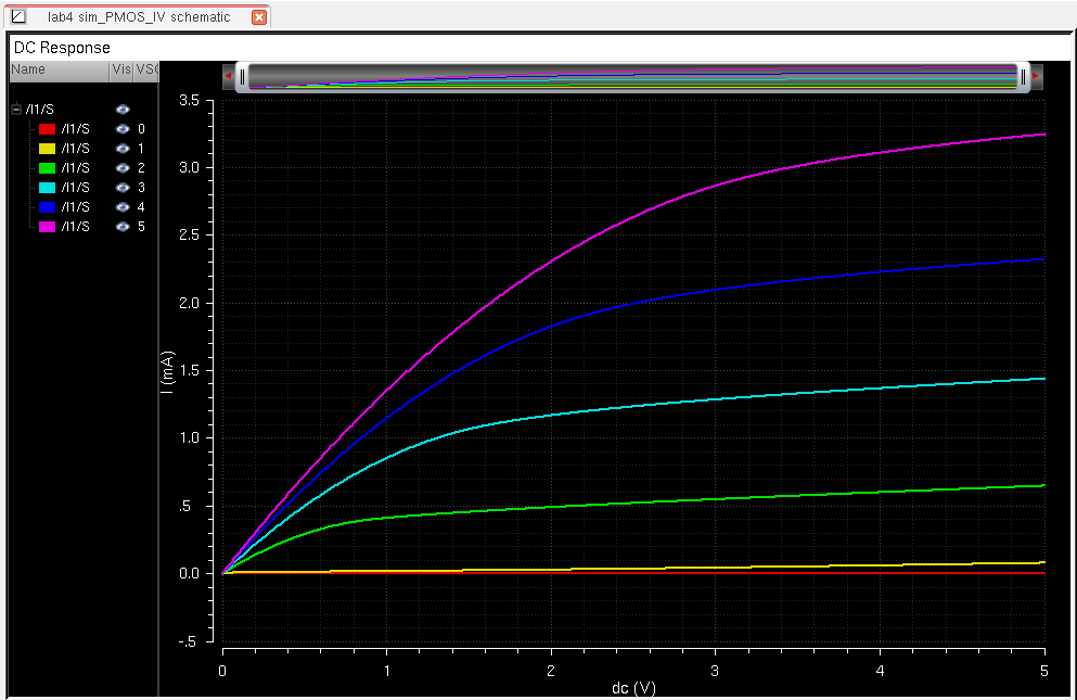
ID v. VSD of an PMOS device for VSD = 100 mV where VSG varies from 0 to 2 V in 1 mV steps.
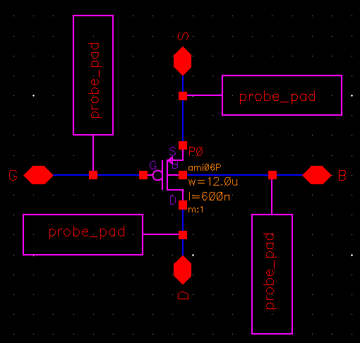
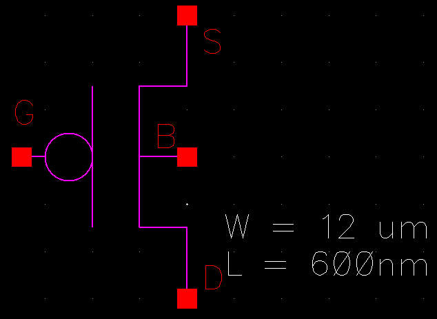
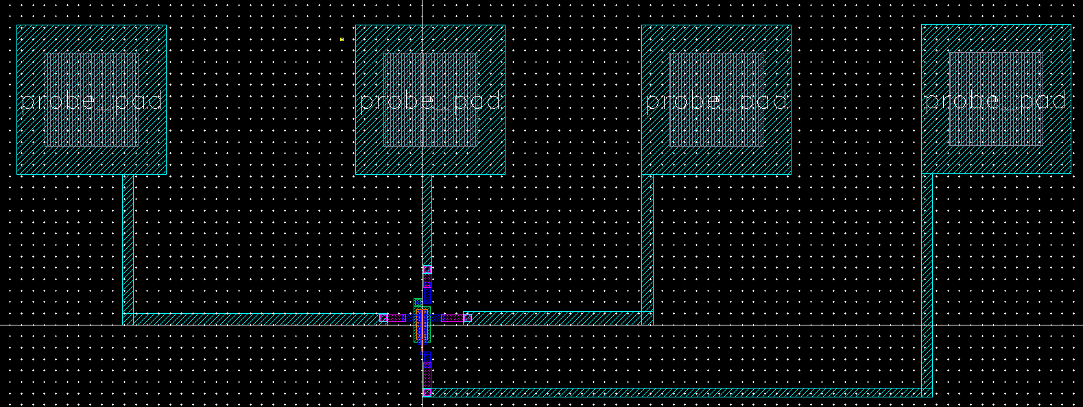
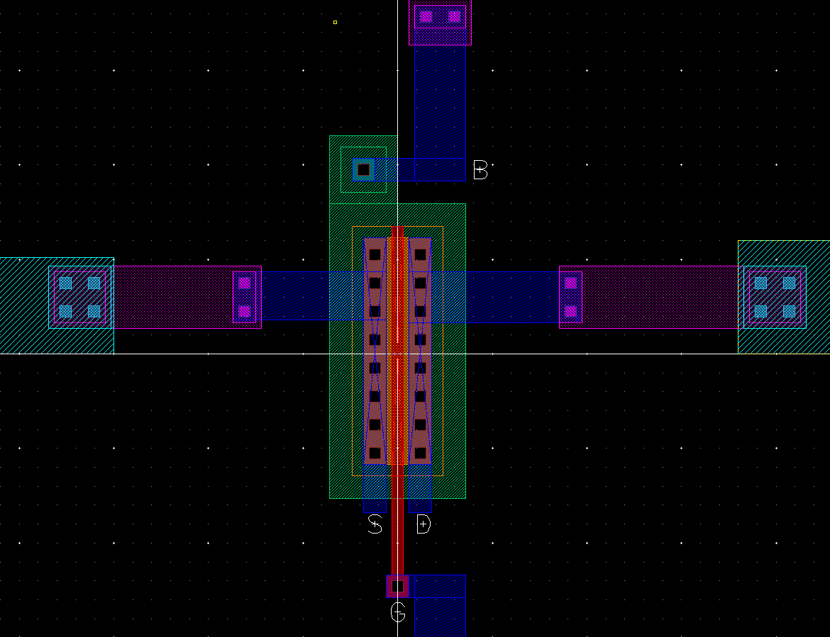
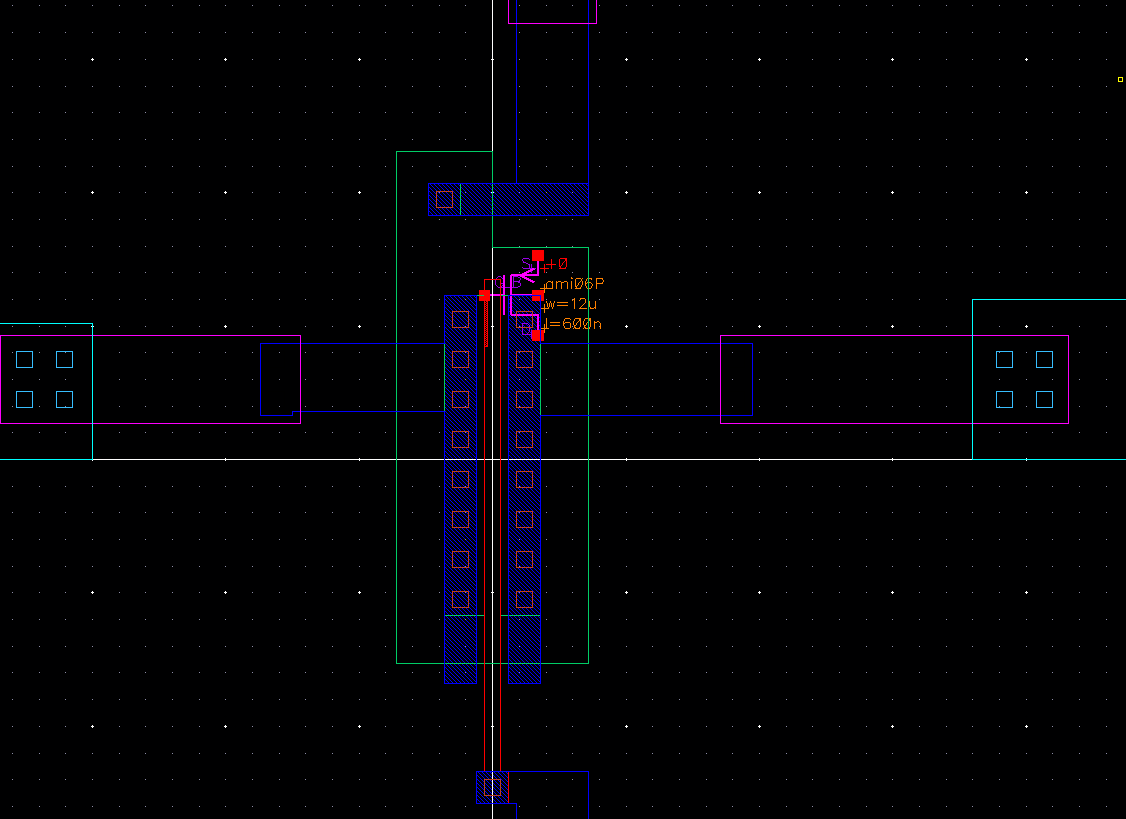
4. Layout of 6u/0.6u NMOS device and connect all 4 MOSFET terminals to probe pads
First we take our NMOS schematic and attach the probe pad symbols we made early,also keeping the same symbol from early.
Then we create a layout of the NMOS with each terminal connected to a probe pad.
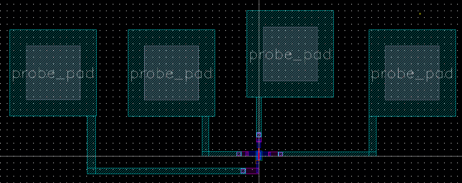
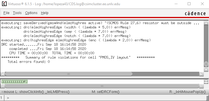
We then DRC, extract, and LVS the layout.
Next we simulate the extracted layout.
5. Layout of 12u/0.6u PMOS device and connect all 4 MOSFET terminals to probe pads
Now we are going to do the same steps for the PMOS device, with the schematic, Layout of the PMOS and symbol.
We DRC, extract, and LVS the layout.
Finally, we simulate the extracted layout.
5. Backing up work
I zipped and emailed a backup of lab 4 to myself.
Go Back to Laboratory reports