Lab 3 - EE 421L Fall 2020
Authored by Abraham Lopez on 09/12/20
Email: lopeza43@unlv.nevada.edu
Design files for lab 3 can be found here.
Lab description
The purpose of lab 3 was to make a layout of the 10-bit DAC using layouts of 10k resistors.
Pre-Lab
The pre-lab involved backing up our previous work and completing tutorial 1.
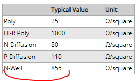
In tutorial 1 we created a layout of a 10k n-well resistor by selecting a length and width that when used in the equation
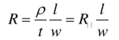
where R square is the sheet resistance, 800 ohms/square, l and w are the length and width of the n-well layer
and R, the resistance, we want to equal 10k ohms.
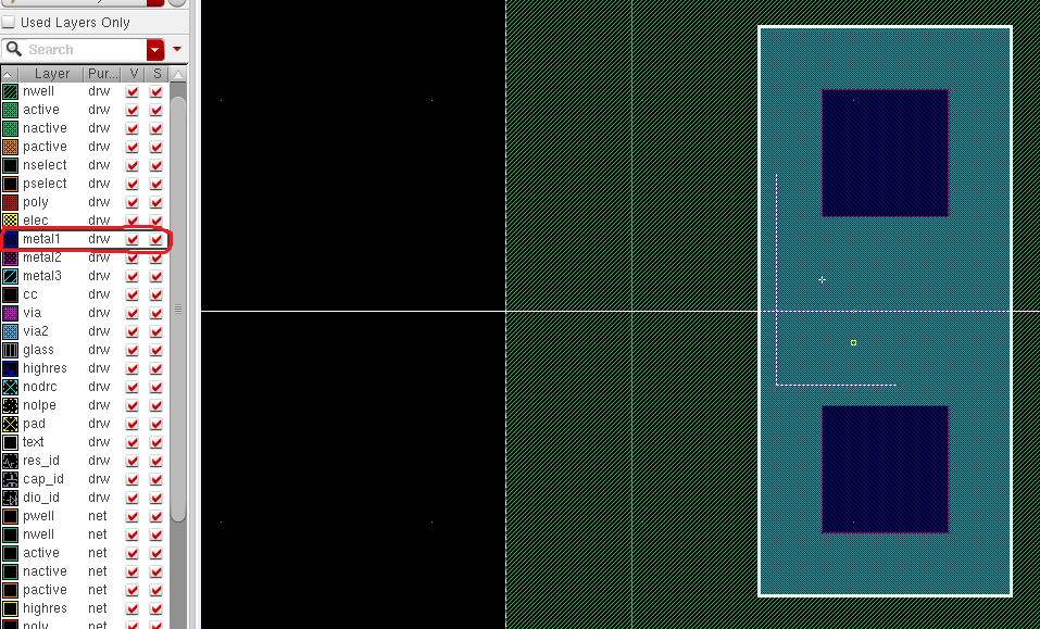
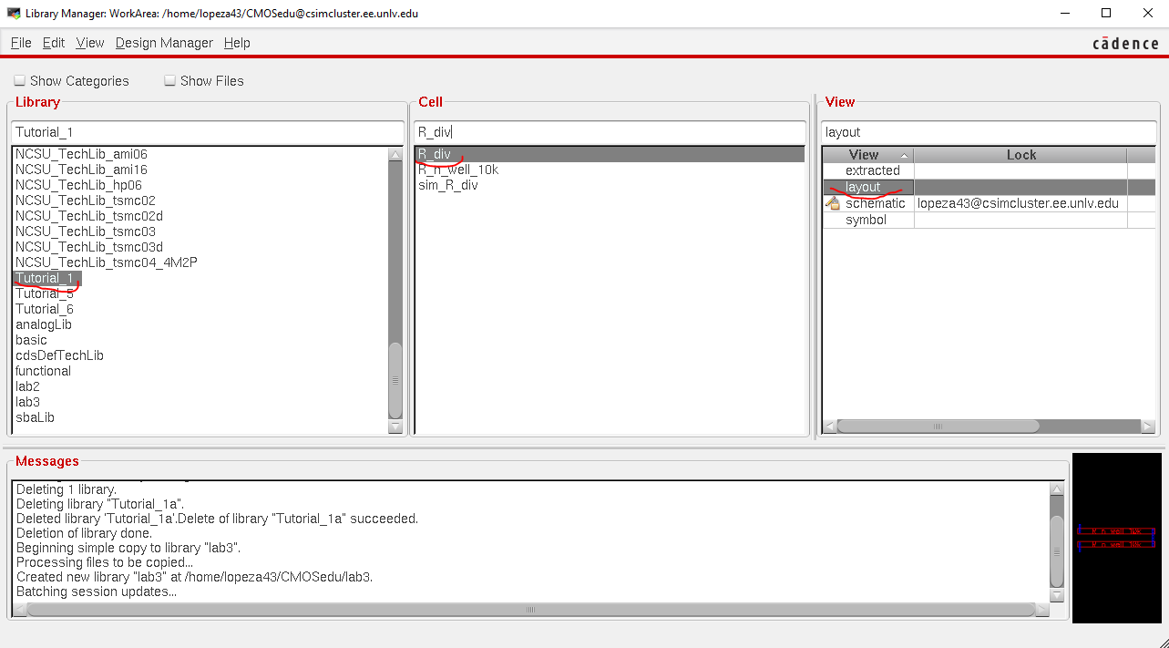
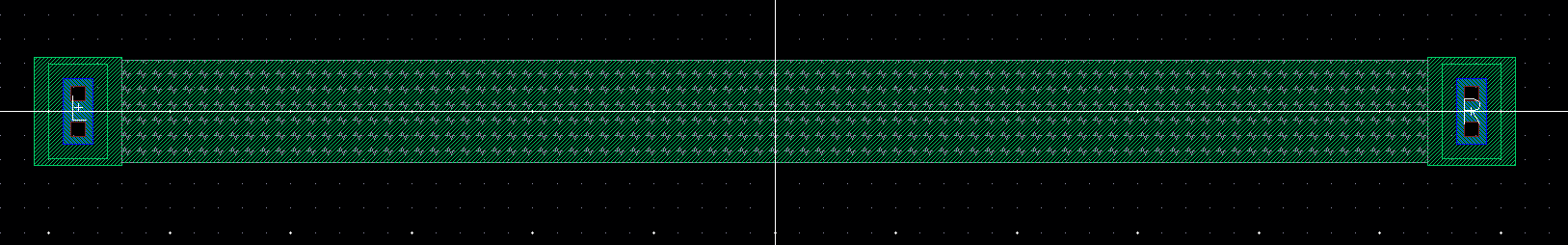
To start off, we first create a new cell in the tutorial 1 library and select it to be a layout.
Then we draw a rectangle using the n-well layer and command "R".
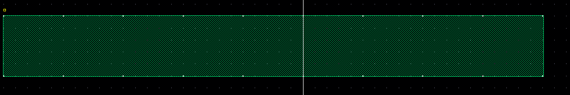
Clicking
on the n-well layer and using the command "q" we can change the
properties of the layer, which include the length and width.
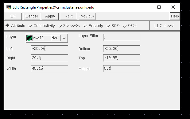
Changing the length and width to 56.1 um and 4.5 um we estimate, using the equation for n-well resistance, that the resistance
should be 10k ohms.
Note:
When selecting values to use for the length and width make sure both
the values when divided by the X snap and Y snap spacing, that a whole
number is given otherwise when we DRC the layout errors will occur
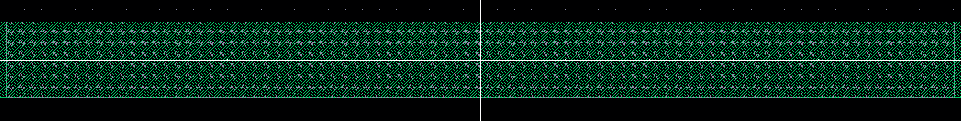
We also want to add ntaps, with 2 rows of contacts, to the end of the n-well layer.
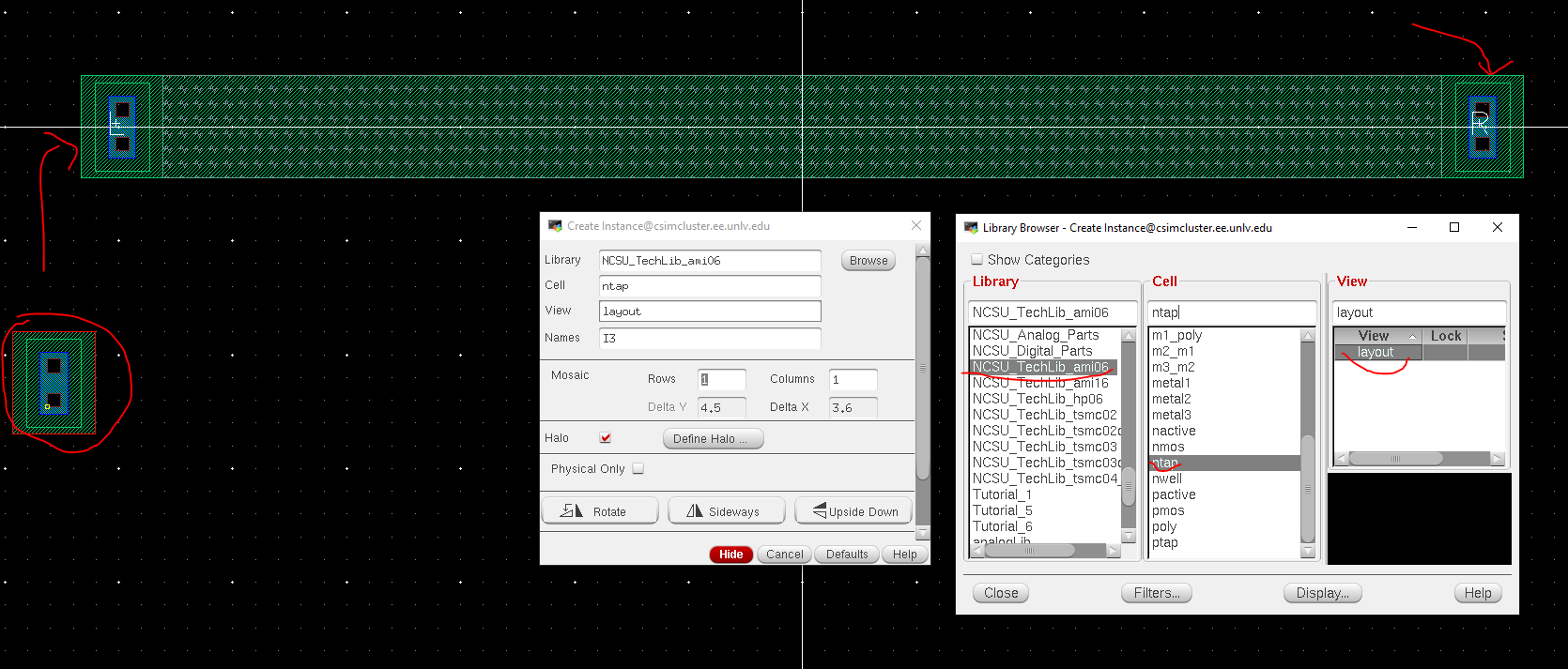
Then add a layer of resistance sheet on top of the n-well layer and also create Pins called L (Left) and R (Right) by
drawing them with a metal 1 layer on the ntap contacts.
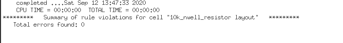
We now want to DRC the layout to make sure there are no errors in our design.
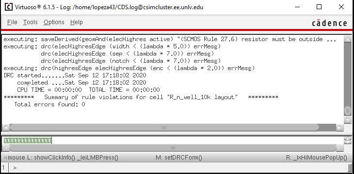
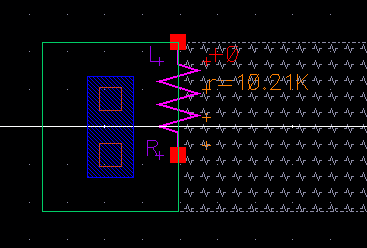
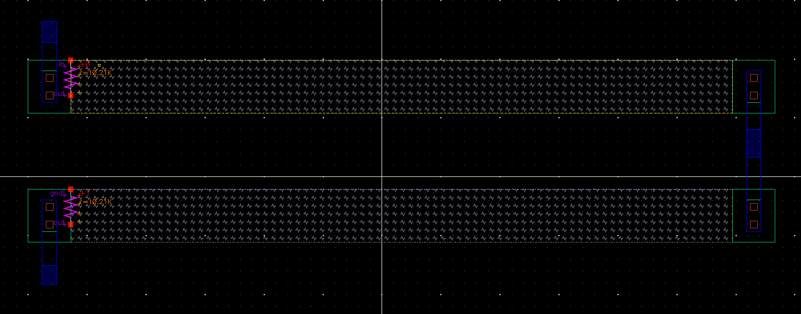
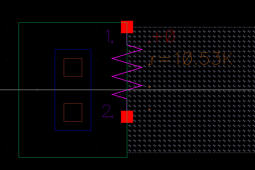
With all of that complete we can extract the layout and verify the resistance labeled which is 10.21k ohms.
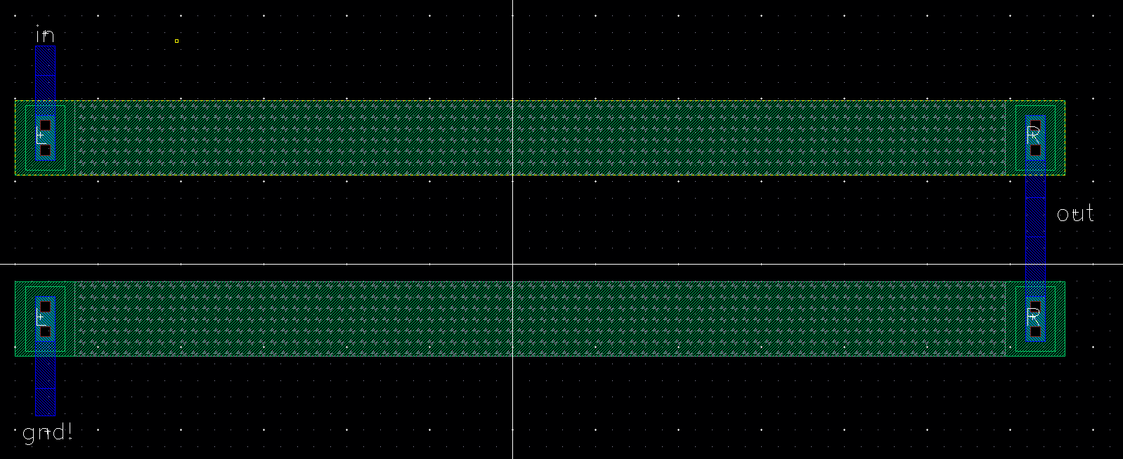
We now have an n-well resistor we can instantiate with "i", so we'll create a new cell layout for the R_div library.
Then
we'll put down two n-well resistors and connect them with metal 1
layers. We also want to create pins of in, out, and gnd! with metal
layer 1.
Next, we want to DRC the design to make sure there are no errors and extract it.
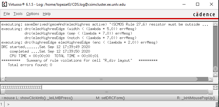
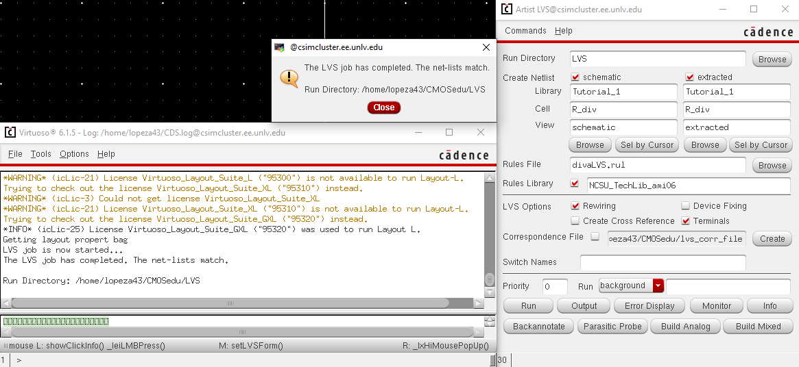
Lastly, we want to LVS the design and that concludes tutorial 1.
Lab Procedures
1. Using the n-well layer to layout a 10k resistor
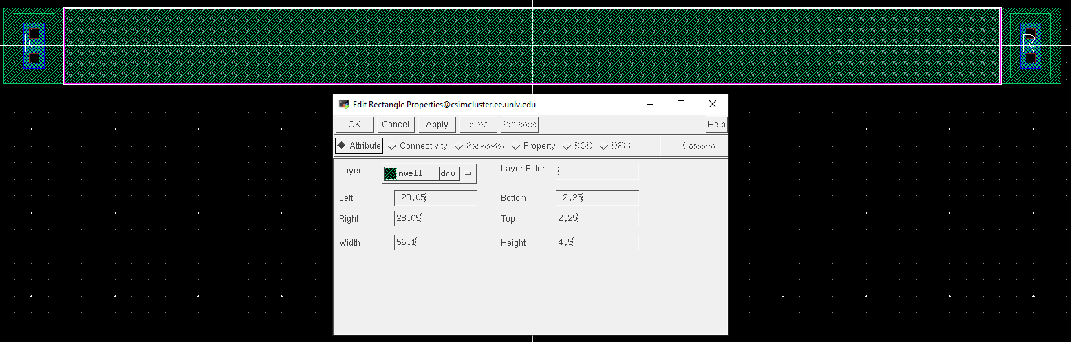
Remembering that to get the resistance of 10k ohms, we need to select a length and width that will give us 10k ohms.
For this we chose a length and width of 54 um and 4.2 um, then plugged them into the equation
and we calculated around 10k ohms.
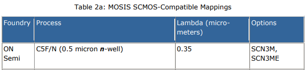
We
also want to keep in mind the MOSIS parameters for the C5 process as
there is a minimum width and the value of the resistance sheet.
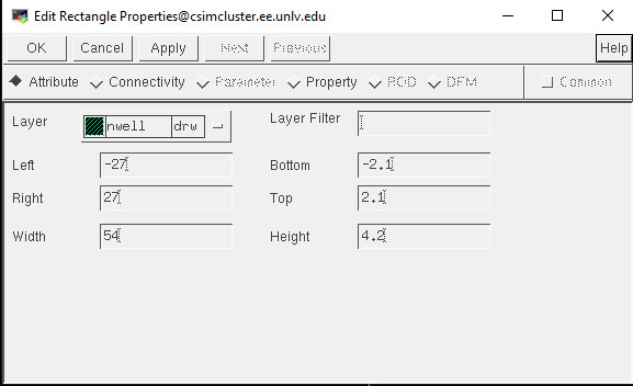
After drawing an n-well and changing the length and width via the properties to 54 um and 4.2 um
We also add the ntaps, pins, and resistance as we did early in the pre-lab.
Next we want to DRC the design and extract the layout to confirm our resistance is around 10k ohms.
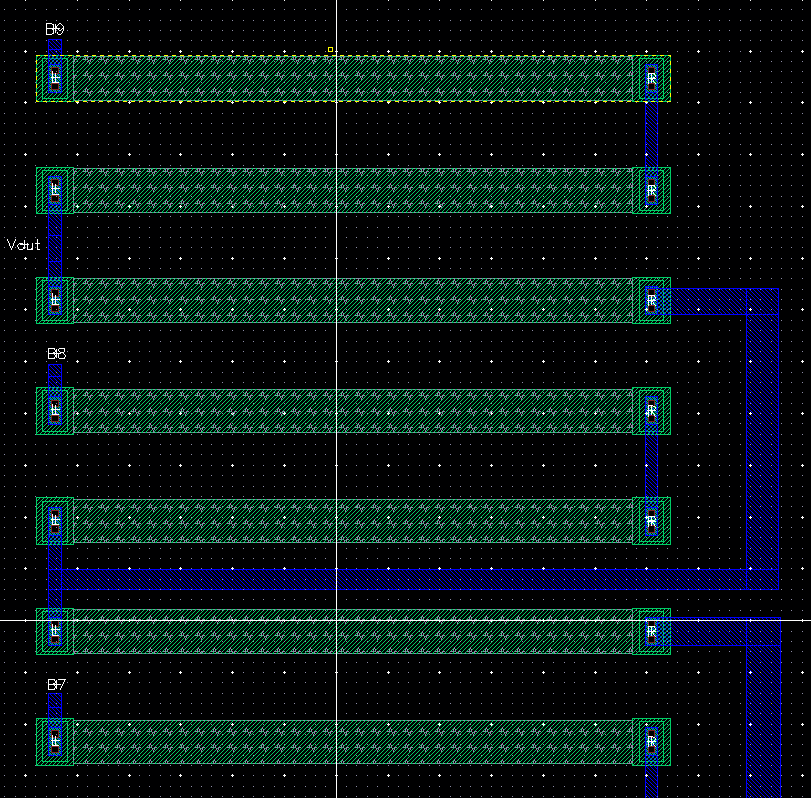
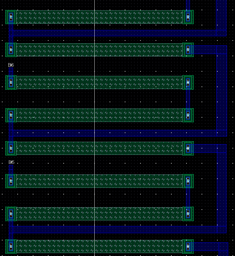
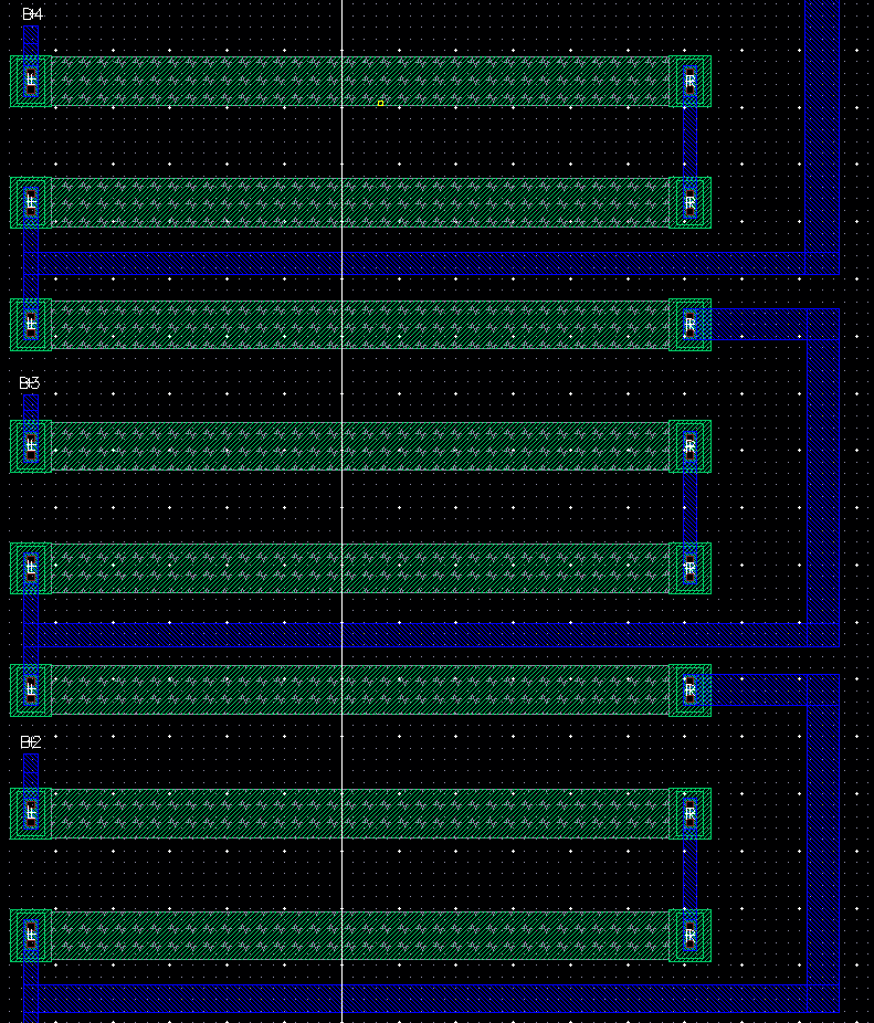
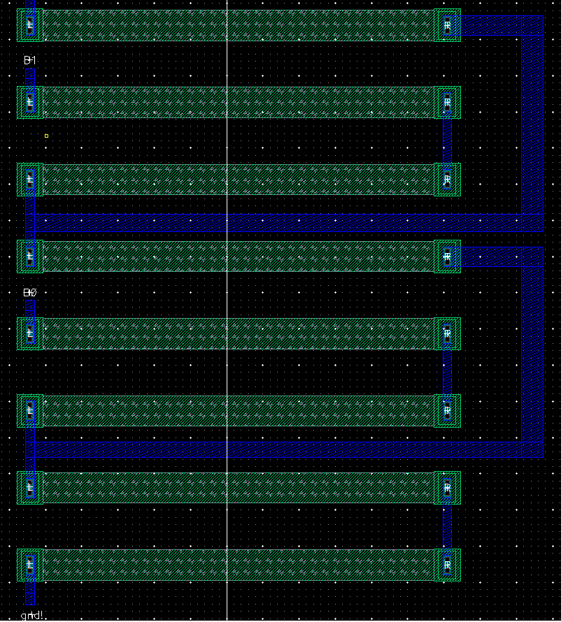
2. Using the n-well resistor to layout the DAC
Now we want to create a layout for the 10-bit DAC based on the schematic below.
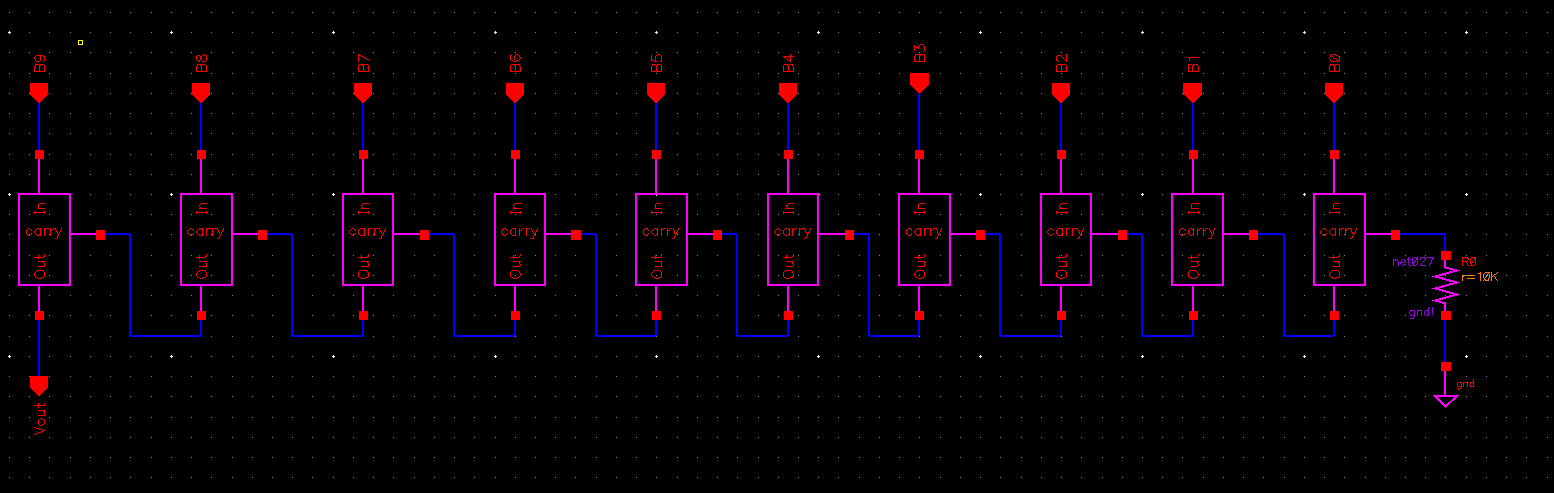
Each block representing a bit is made of three resistors and there is 10 blocks along with 1 10k resistor at the end. Which
means
that for the layout we need 31 n-well resistors. All of them need to
wired similar to the schematic for the DAC with the carry connecting to
the output also creating pins for all the inputs, outputs and gnd!,
which can be seen below.
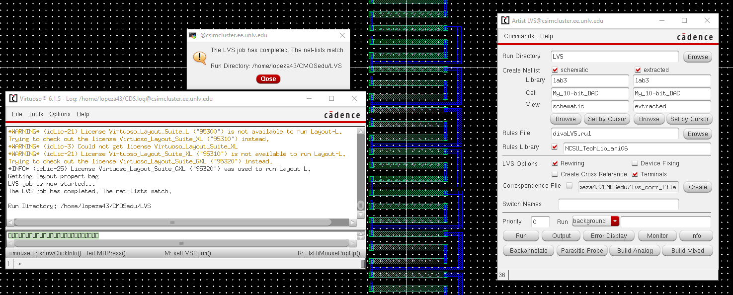
We then DRC and extract the design.
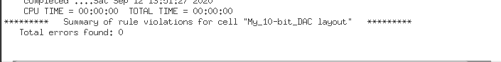
Lastly, LVS the design to make sure the net-list matches
3. Backing up work
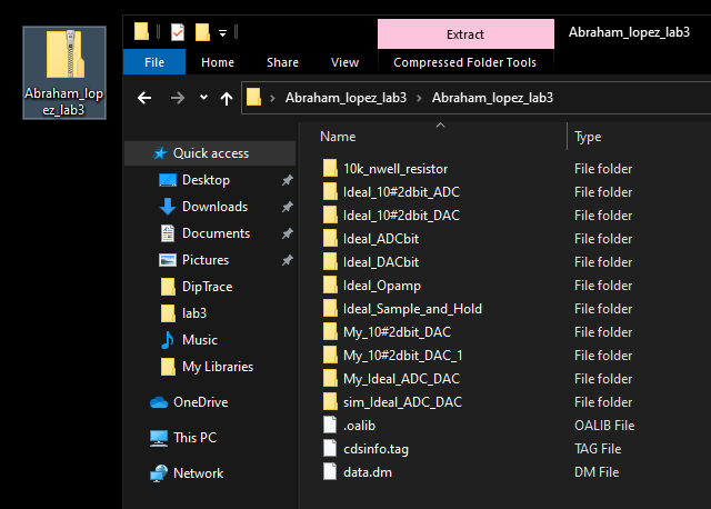
I then backed up my files by zipping them and emailing them to myself.
Design files for lab 3 can be downloaded here.
Go Back to Laboratory reports