Digital Receiver
Authored
by Peter Kim
kimj98@unlv.nevada.edu
11/18/2020
Project:
Design, layout, and simulate a digital receiver circuit that accepts a
high-speed digital input signal D and Di (a differential pair) in C5
process. Use table to summarize your design's performance.
ex) D = 5V, Di = 0V, OUTPUT = 1
ex) D = 1V, Di = 2V, OUTPUT = 0
Design based on the parallel self-biased differential amp topology seen in Fig. 18.23 seen below.

Design
goal: Design for high-speed and low-power digital receiver circuit.
Characterize your design (in sims) and the trade-offs.
One
good practical application for this circuit is for Ethernet cable
switch. There are twisted pairs of wires inside Ethernet cable that
sends differential pair of 1's and 0's from a modem. When you run
Ethernet cable a long distance from the modem the signal levels drop
and gets weak at the receiving end. In order to solve this problem, a
digital receiver is used to regenerate the signals back to its full
digital levels.
Minimum design
specification: Using C5 process, 250 Mbits/s (a bit width of 4 ns) with an
input voltage difference of 250mV (D and Di swinging between 2.75V and
3V)
| Speed | Bit width |
| 200 Mbits/s | 5 ns |
| 250 Mbits/s | 4 ns |
| 333 Mbits/s | 3 ns |
| 500 Mbits/s | 2 ns |
| 1 Gbit/s | 1 ns |
C5 Model design parameter
| Technology | Rn | Rp | Scale Factor | Cox = C'ox* WL*(scale)^2 |
| C5 | 20k*(L/W) | 40k*(L/W) | 300nm | (2.5fF)*WL |
C5 Process switching resistances and oxide capacitances
| C5 Process | Drawn | Scale factor | Actual size | Rn,p | Cox,n,p |
| NMOS | 20/2 | 300nm | 6μm by 0.6μm | 2k | 9fF |
| PMOS | 40/2 | 300nm | 12μm by 0.6μm | 2k | 18fF |
PART 1 : Schematic
Inspection of NMOS INPUT BUFFER with 6μ/6μ MOSFETs and a inverter with 12μ/6μ MOSFETs with D and Di swinging between 2.75V~3V @250Mbit/s.

Simulation Plot for D and Di swinging between 2.75V~3V @250Mbit/s:
| bit width of '0' | 3 ns |
| bit width of '1' | 3.1ns |
| VPLH | 764ps |
| VPHL | 570ps |
Setting this plot as a benchmark, we will change different parameters to see the limitation of NMOS BUFFER.

Simulation table for D and Di swinging between 2.75V~3V @250Mbit/s
(note: power measured from 5ns~40ns to neglect initial charge):
Tradeoff: as you increase length of LONG L (from schematic), it consumes less power but causes longer delay.
Variations of bit width of '0' and '1' gets larger as you increase length of LONG L.
Conclusion: making bottom NMOS (LONG L) weaker, increases resistance causing to consume less power but slower response.
| Change in LONG L | Vplh | Vphl | bit width '0' | bit width '1' | Power consumption (AVG) | Power consumption of LONG L |
| 600nm (minimum) | 764ps | 570ps | 3ns | 3.1ns | 5.45 mW | 731 μW |
| 3μm | 1.33ns | 544ps | 2.59ns | 3.34ns | 3.37 mW | 466 μW |
| 6μm | 1.77ns | 640ps | 1.97ns | 3.14ns | 2.79 mW | 328 μW |
| 9μm | 2.15ns | 687ps | 1.27ns | 3.44ns | 2.54 mW | 257 μW |

Simulation table for D and Di swinging between 2.75V~3V @250Mbit/s with length of Long L of 4.5 um: | Change in Bit width | Vplh | Vphl | bit width '0' | bit width '1' | Power consumption (AVG) |
| 5n | 1.55ns | 578ps | 4.51ns | 3.4s | 2.90 mW |
| 4n | 1.57ns | 577ps | 2.9ns | 3.7ns | 3 mW |
| 3n | 1.55ns | 577ps | 2.68ns | 1.69ns | 3.12 mW |

Simulation table for D and Di swinging between 2.75V~3V @250Mbit/s with length of Long L of 4.5 um:
| Change in rise and fall time | Vplh | Vphl | bit width '0' | bit width '1' | Power consumption (AVG) |
| 2ns | 1.73ns | 590ps | 2.63ns | 4.21ns | 2.97 mW |
| 1ns | 1.57ns | 577ps | 2.9ns | 3.7ns | 3 mW |
| 500ps | 1.49ns | 540ps | 2.8ns | 3.1ns | 3.01 mW |

Simulation table of varying input voltage @250Mbit/s with length of Long L of 4.5 um:
| Change in Input range | Vplh | Vphl | bit width '0' | bit width '1' | Power consumption (AVG) |
| 2.75V~3V | 1.57ns | 577ps | 2.9ns | 3.7ns | 3 mW |
| 1.5V~1.75V | 1.89ns | 1.17ns | 2.3s | 3.37ns | 2.11 mW |
| 0.5V~0.75V | n/a | n/a | n/a | n/a | n/a |

Temperature Sweep plot: temperature from 0°C to 100°C, you
can observe that as temperature rises bit length of '1' shrink and bit
length of '0' expands this is true for all input ranges and for
different parameters.

From the simulation of NMOS buffer, the length of LONG L should be between 3μm~6μm (selected 4.5μm for my design).
NMOS buffer is used for higher input signal (greater than Vthn), and PMOS buffer is used for smaller signals (close to gnd)
PMOS buffer is complementary of NMOS buffer, putting 2 buffers in parallel will cover wide range of signal.
When signal is close to gnd, NMOS buffer will shut off.
When signal is close to vdd, PMOS buffer will shut off.
Base circuit based on topology seen in fig 18.23.
6μ/6μ MOSFETs and a inverter with 12μ/6μ MOSFETs with D and Di swinging between 2.75V~3V @250Mbit/s.
Base schematic plot: note Vout does not swing to vdd, buffer needs adjustment.

DC sweep to find gain (using LT spice):

Schematic & Plot for gain using LTspice (note: 10pF and 10M load is for probe set up)

DC sweep:

Gain Plot: neglecting very low and very high signals, the lowest gain is about 40.
The minimum required voltage difference is 250mV, gain of 40 is enough to cover the voltage difference of 125mv.
Therefore, single stage buffer is adequate for my design.
However,
cascading 2 or more BUFFER is desired for more robust performance (very
low voltage difference) for a wide range of input signals at cost of
layout space.

Probe setup: Assuming this design is to be fabricated, the design needs to drive 10pF of capacitance for probe setup for testing its operation.

FINAL DESIGN
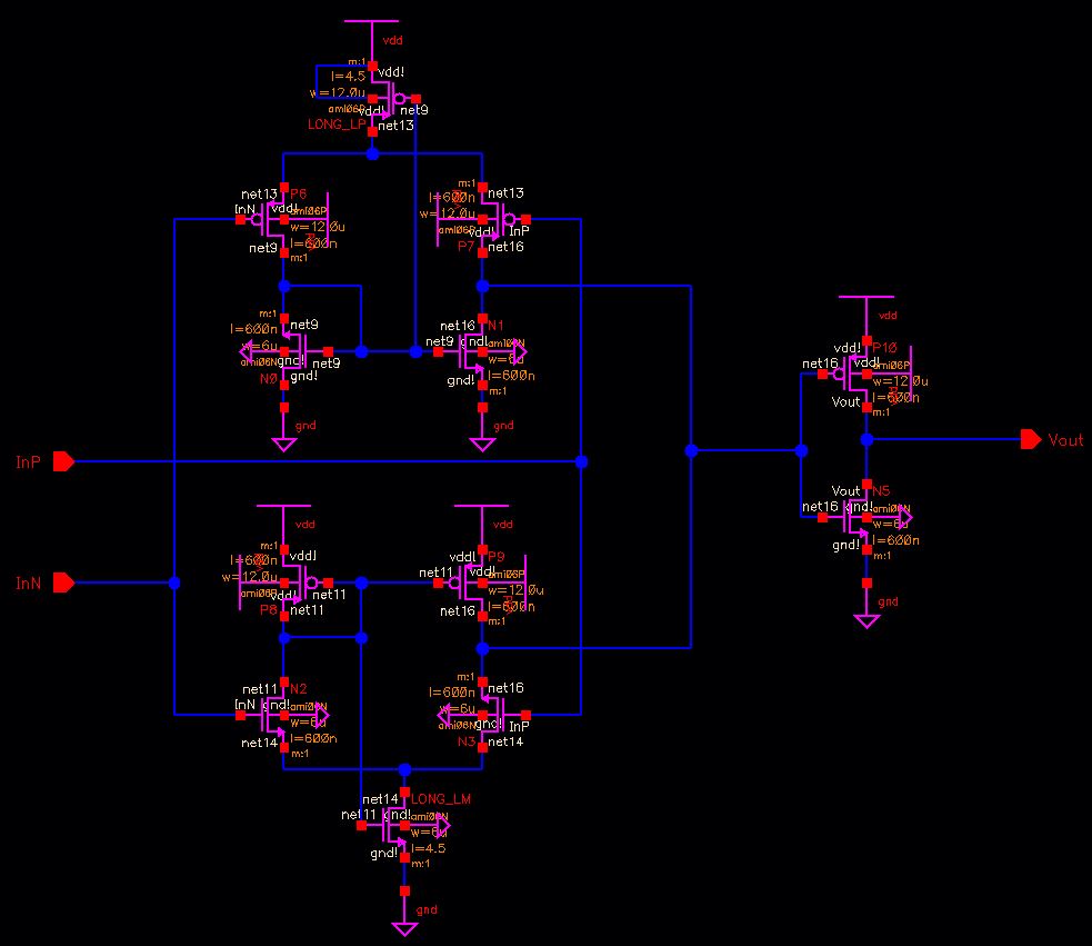
Schematic of diff-amp:

Schematic of buffer

Schematic of design:

Simulation schematic:

Simulation Results:
Temperature sweep: input 2.75V~3V @ 250Mbit/s

Simulation table for D and Di swinging between 2.75V~3V @250Mbit/s with length of Long L of 4.5 um: | Change in Bit width | Vplh | Vphl | bit width '0' | bit width '1' | Power consumption (AVG) |
| 5n | 1.05ns | 1.22ns | 6.27ns | 5.85s | 3.71 mW |
| 4n | 1.05ns | 1.22ns | 4.9ns | 5.0ns | 3.84 mW |
| 3n | 1.05ns | 1.23ps | 3.77ns | 4.14ns | 4.11 mW |

Simulation table for D and Di swinging between 2.75V~3V @250Mbit/s with length of Long L of 4.5 um:
| Change in rise and fall time | Vplh | Vphl | bit width '0' | bit width '1' | Power consumption (AVG) |
| 2ns | 1.21ns | 1.35ps | 6.1ns | 5.8ns | 3.86 mW |
| 1ns | 1.05ns | 1.22ns | 4.9ns | 5.0ns | 3.84 mW |
| 500ps | 988ps | 1.17ns | 4.3ns | 4.8ns | 3.95 mW |

Simulation table of varying input voltage @250Mbit/s with length of Long L of 4.5 um:
(note that lower input didn't work, which is consistant with gain plot above)
| Change in signal range | Vplh | Vphl | bit width '0' | bit width '1' | Power consumption (AVG) |
| 2.75V~3V | 1.05ns | 1.22ns | 4.9ns | 5.0ns | 3.84 mW |
| 1.5V~1.75V | 1.5ns | 956ps | 5.6s | 4.29ns | 3.78 mW |
| 0.5V~0.75V | n/a | n/a | n/a | n/a | n/a |

Simulation table of varying input voltage @250Mbit/s with length of Long L of 4.5 um:
| Change in VDD | Vplh | Vphl | bit width '0' | bit width '1' | Power consumption (AVG) |
| 5V | 1.05ns | 1.22ns | 4.9ns | 5.0ns | 3.84 mW |
| 4V | 931ps | 1.83ns | 4.0ns | 6.05ns | 1.77 mW |
| 3V | n/a | n/a | n/a | n/a | n/a |

Simulation with random pulse width, rise time, and sequence:

END of Part 1
PART 2: Layout
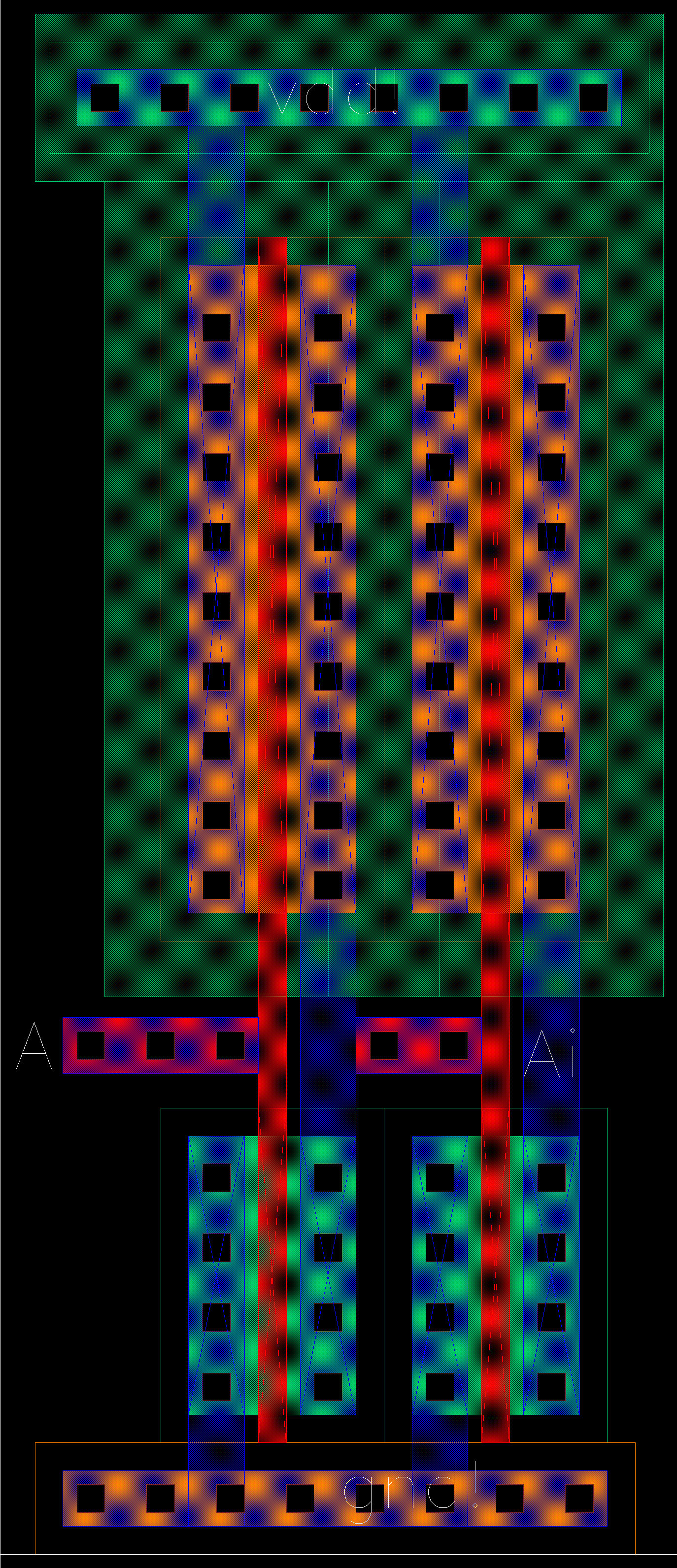
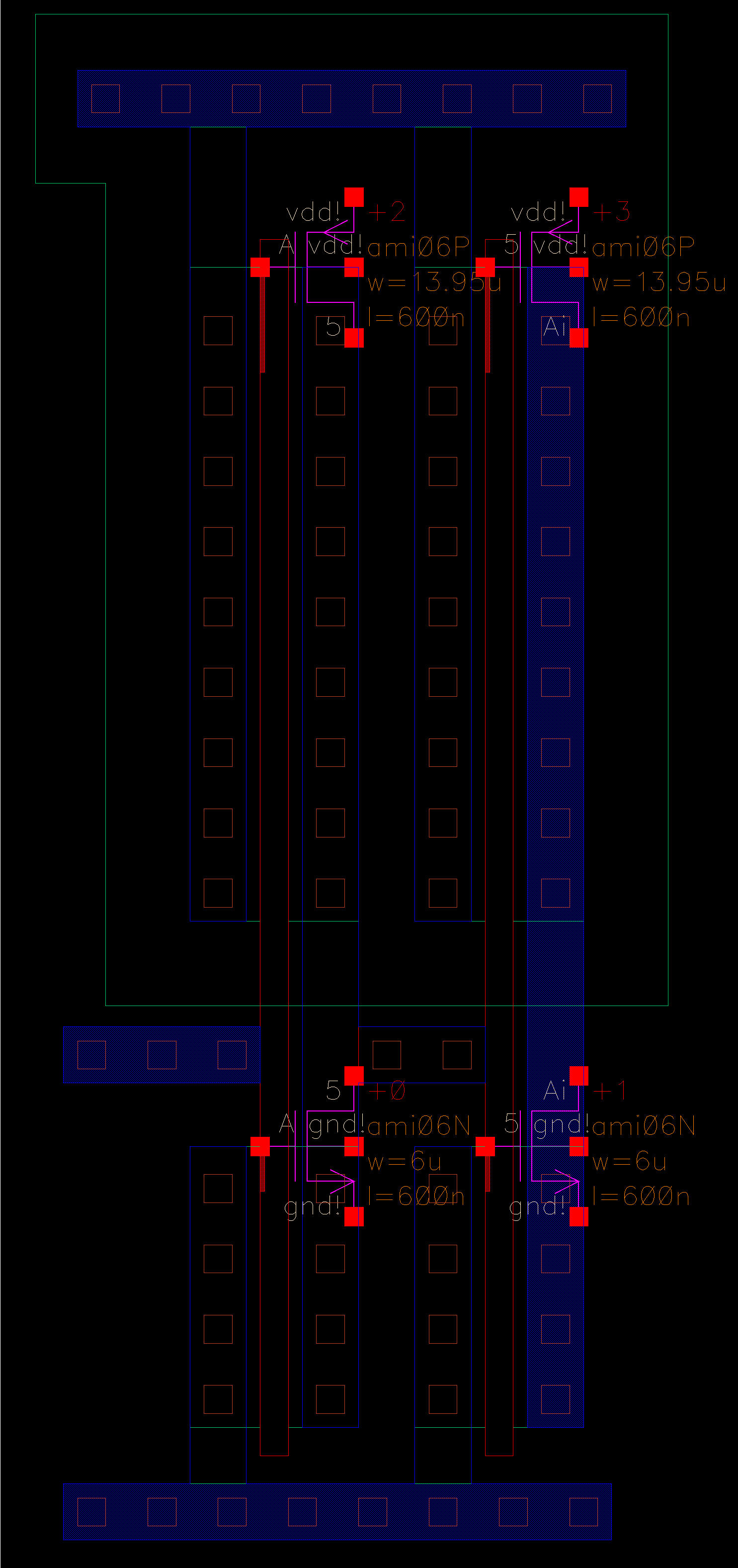
Layout & extracted view of output buffer (click for a larger image):


Output buffer cells DRC and LVS without error shown below:


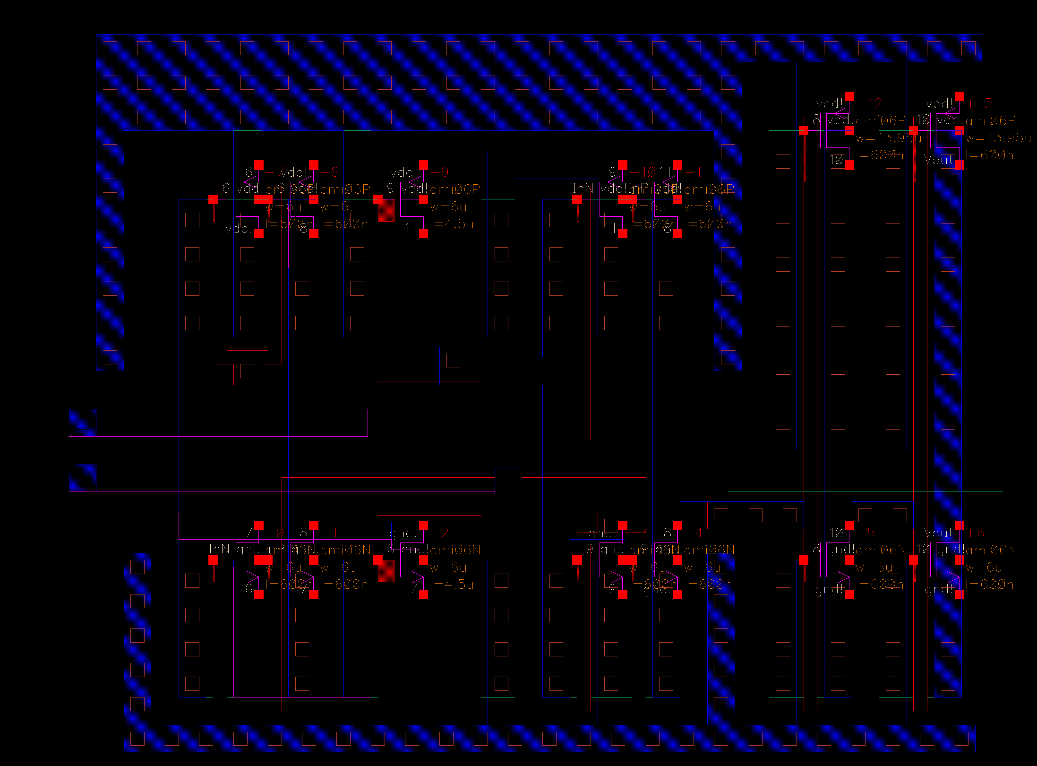
Layout & extracted view of Diff-AMP (click for a larger image):


Diff Amp cells DRC and LVS without error shown below:


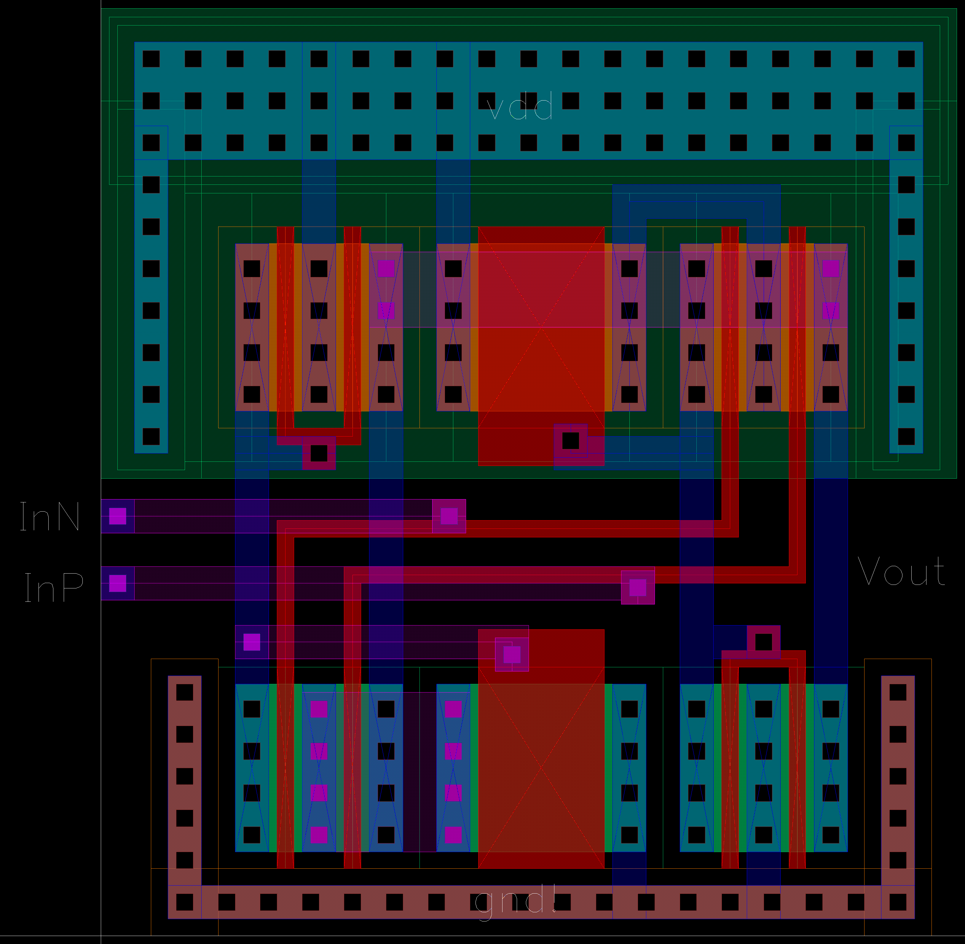
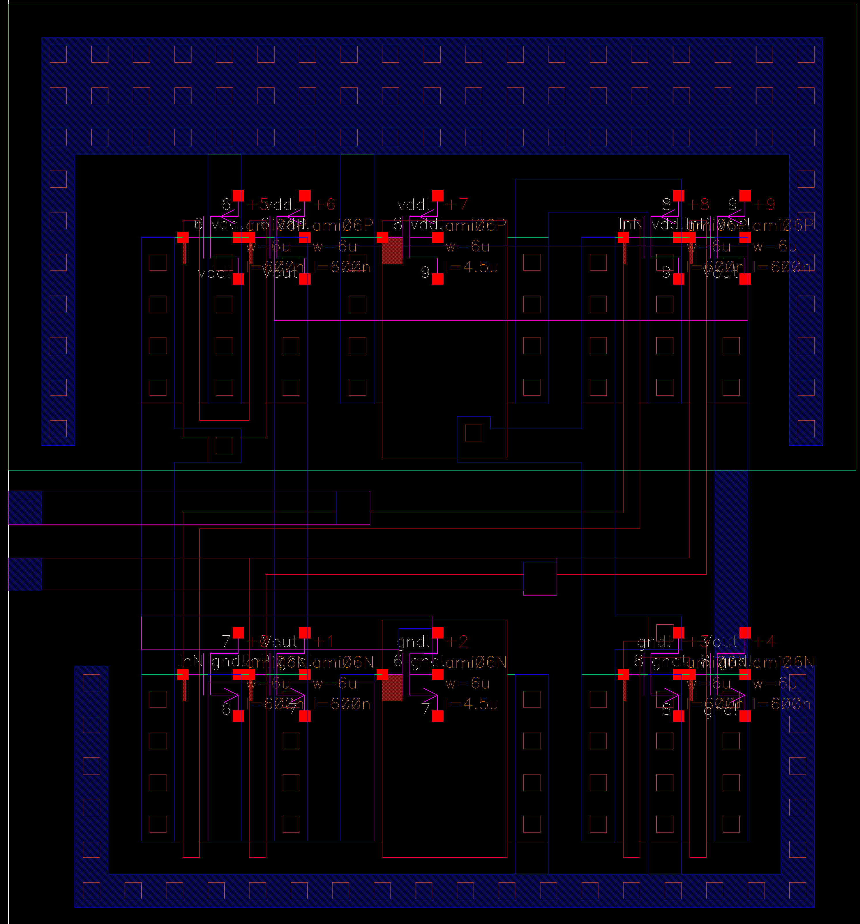
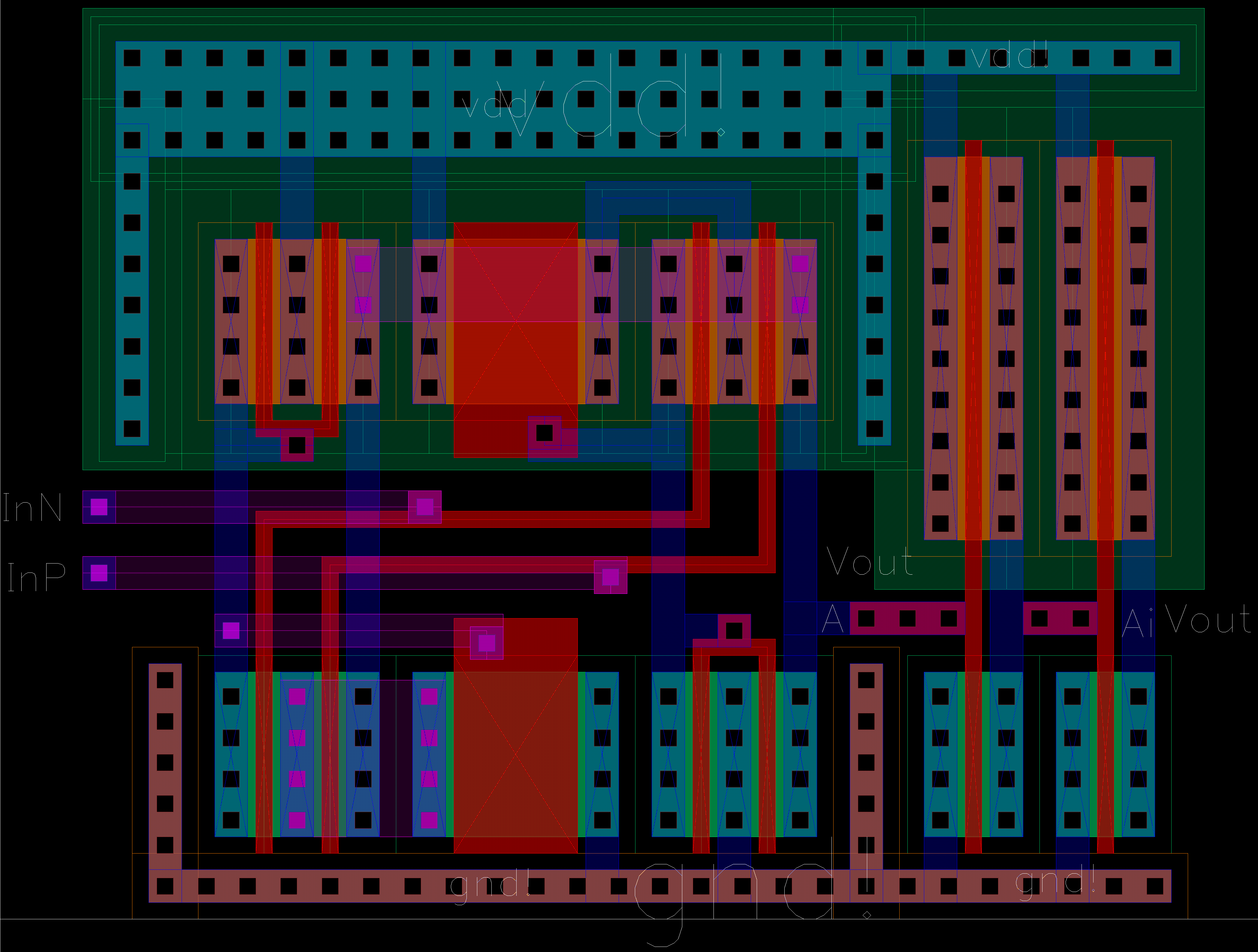
Layout & extracted view of Digital Receiver:


Digital Receiver cells DRC and LVS without error shown below:


Extracted cell simulation (solid lines represent schematic view & dotted lines represent extracted view):


END of Part 2
Click here for project files (lab_project.zip)
Return
to EE 421L
Labs