Lab Project - ECE 421L
For this lab project, the digital reciever will be based on the topology seen in fig 18.23. This figure shows 2 self biasing diff amps in both the NMOS and PMOS version of the diff amps. These two different diff amps are connected together and outputs are tied and go into an inverter. Using both diff amps gives better results as both the delays are considerably better than using just one. The PMOS and NMOS combination also get rid of an offset on the output based on the Vm and Vp of the circuit. We need a fast operating reciever that can operate in the ranges of 2.75V and 3V. To start, the two self biasing circuits need to be created. A standard 12u/0.6u for the PMOS and 6u/0.6u for the NMOS with be used throughout the circuits.
Figure 1 - NMOS Self Biasing Diff Amp

Figure 2 - PMOS Self Biasing Diff Amp
Now that the two diff amps are created, the reciever can be put together. A symbol will be created for both the diffamps and used in the schematic of the reciever.

Figure 3 - Digital Reciever Schematic
We can see in the schematic that the PMOS and NMOS diff ampa are connected together in a parallel fashion with two inverters on the outputs of the diff amps. The two inverters are needed instead of one to give a better output in the sim by correctly showing if D > Di then the output should reach a logic high. With two inverters theres an increase in the use of power but it creates a better output. After this schematic is made, a symbol can be created in it and we will use this symbol to simulate the function of the reciever.

Figure 4 - Digital Reciever Symbol

Figure 5 - Digital Reciever Sim
We can see in the sim there is an added 1K load on the output of the digital reciever, this is to test the circuit's function in a case where there is likely to be a small resistive load on the output instead of just no connection. This should yeild simulation results that are more accurate in a real setting. Later, the resistive load will be swept to see the differences in output as well as how a capacative load would affect the digital reciever as well. We will first start with a simulation of a frequency of 100Mhz for the two differential input signals.

Figure 6 - Digital Reciever Simulation Graph with 100Mhz Frequency Input
In this graph we can see that the inputs are swinging back and forth from 2.75V to 3V. We can also see that the correct outputs are there as when D > Di then the output is 1 while Di > D causes a output of 0. The receiver is taking the input values, amplifying the values and translating them into readable logic levels. Given the resitive load, we can see than the output logic levels are decent going from 0 to 2.5, about half of the VDD. We can also see in the graph, the bit width being that of 4ns as state as one of the goals of the project but still the Mbit/s here is 100. Now it's time to test the the circuit at higher frequencies.

Figure 7 - Digital Reciever Simulation with 200Mhz Frequency
In this graph the frequency was raised up to 200Mhz and we can see that the output maintains its max vout but the curve is more rounded with a less stable bit width. The bit width has also decreased being at around 2.5ns width. We will now try the 250Mhz frequency.

Figure 8 - Digital Reciever Simulation with 250Mhz Frequency
The top of the vout curve is even more rounded and the bit width has decreased but the circuit is able to still output a high enough logic signal.
We can now test the differences in power dissapation throughout this circuit as the circuit takes on higher speed inputs. This can be based on the Dynamic Power Disappation from inverters given by the equation:
PAvg = VDD*IAvg = CTot*VDD^2*fclk
This equation shows that the inverter will disappate more power as the frequency of the clock input increases. Seeing that the circuit has 2 inverters and including the disappation of power in the diff amps we can say for certain that the circuit should disappate more power as the speed of the circuit increases. There are adjustments that can be made to mosfet sizing and current to increase the speed but there is a tradeoff to speed and gain and we need the output levels to be high and use less power.

Figure 9 - Power Disappation with 100Mhz Input

Figure 10 - Power Disappation by 200Mhz Input
Using these two provided graphs we can see that frequency of power disappation increases with the frequency of the input. As higher and higher frequencies are used then the circuit starts to burn more and more power as it starts to work the higher speed inputs.
The circuit should now be tested with different temperatures. A parametric graph with the temperatire being swept up will be created. This should show how the circuit will react at different temperatures.

Figure 11 - Digital Reciever Temperature Sweep
We can see that the circuit stating at the lowest temperature which is red and going down. As the temperature increases the circuit's output voltage starts to decrease but we can see that the circuit still maintains a decent logic high output.
Now the VDD of the Circuit will be swept and we will do it in 1 V increments starting at 5.

Figure 12 - Digital Reciever VDD at 4V
Since we've already seen the circuit working at a VDD of 5 this graph shows the circuit with a VDD of 4. We can see that the logic high output of the circuit has dropped. We can expect the output to drop even more as the VDD goes down.

Figure 13 - Digital Reciever at 3 VDD
The output has dropped significantly with a VDD of 3V.

Figure 14 - Digital Reciever at 2VDD
At this point the circuit has stopped working with a VDD of 2 and thus shows that the limit of the circuit is somewhere above 3V to 5V. It is also important to note that the load of 1K stays on the circuit throughout the simulations of temp and vdd changing.
Now that the circuit has been tested with different temperatures and VDD we can also test with different loads but first we should see the circuit without any load and how it functions.

Figure 15 - Digital Reciver with no Load
No Load on the circuit shows that it works perfectly, with no load the output of the circuit goes to its max that it can get. We get full output logic with no load on the circuit. We can also see that the curvature of the top portion of the output voltage is more stable.

Figure 16 - Digital Reciever Resistive Load Sweep
The resistive loads on the circuit show that more resistance will decrease the output voltage and up to a certain point, a high enough resistive load would cause the circuit to malfunction unless we increase the strength of the reciever to have more gain. This resistive sweep shows that the circuit can work thorughout the different resistive loads.
We can now try seeing what a capactive load would do to the circuit and sweep it at different values as well.

Figure 17 - Digital Reciever with Capacitive Load Sweep
We can see that the capacitive load will start to change the output wave from to be more triangular like. We can also see that the ciruit with a capacitive load seems to maintain the maximum output high of around 5V.
Layout of the Digital Reciever:
Now that all the simulations show the circuit is working fine we can start on the layout of the circuit. To make this layout as easy as possible we will first layout the PMOS and NMOS diffamps separately then connect everything together in the end on one layout.

Figure 18 - NMOS Diff Amp Layout

Figure 19 - NMOS Diff Amp DRC
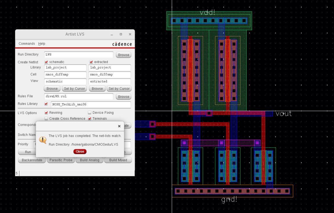
Figure 20 - NMOS Diff Amp LVS
After finishing the layout of the NMOS diff amp and successfully doing the DRC and LVS of the circuit we can move onto the PMOS Diff Amp.
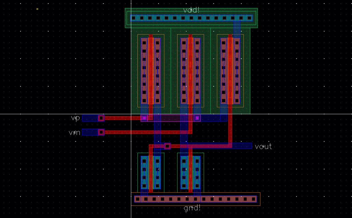
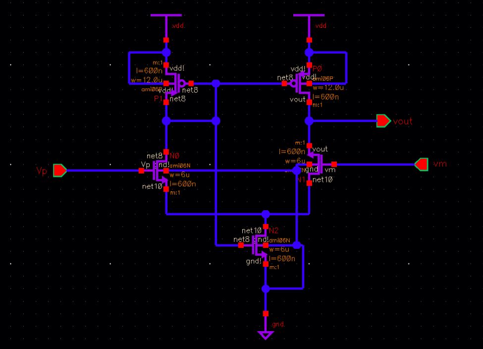
Figure 21 - PMOS Diff Amp Layout
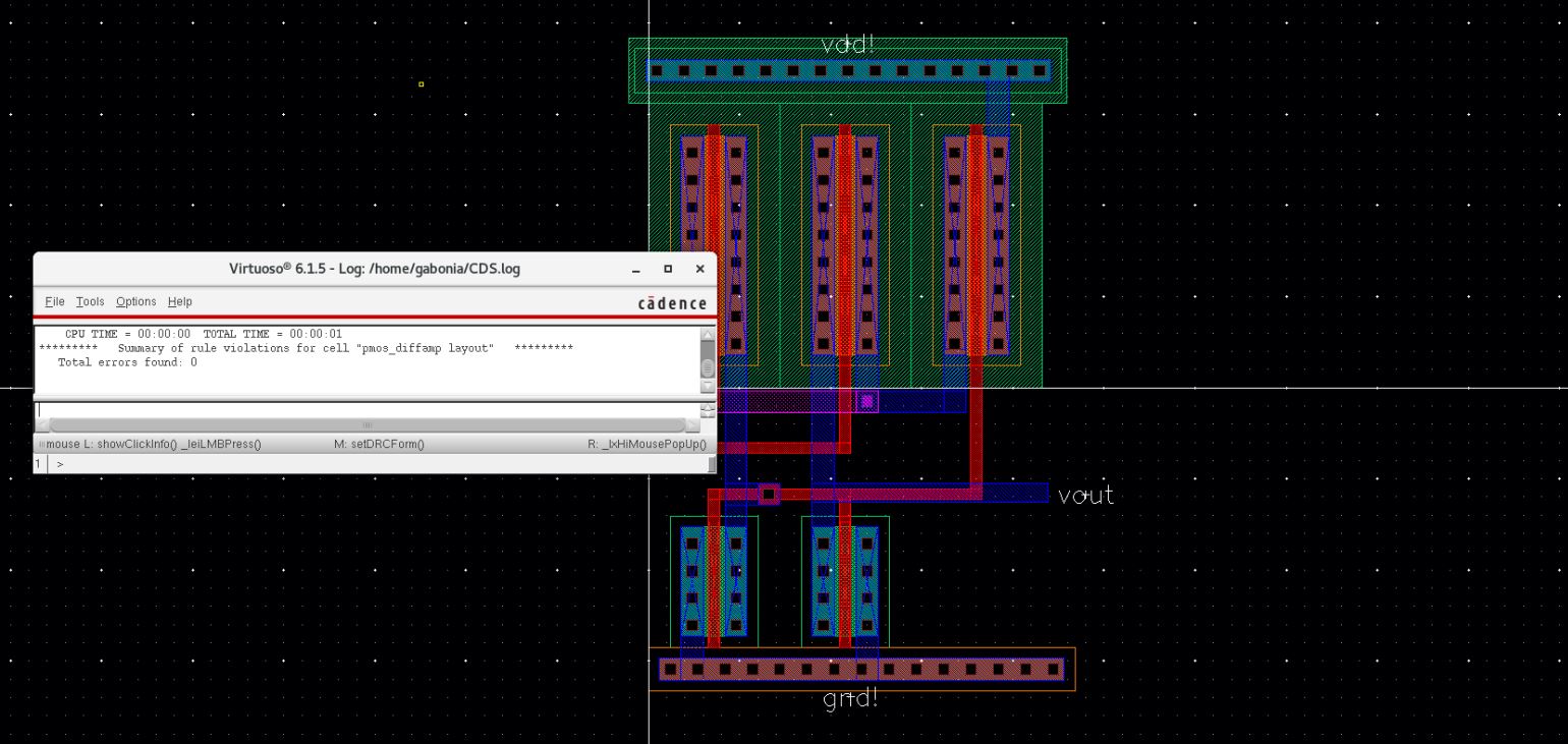
Figure 22 - PMOS Diff Amp Layout DRC
Figure 23 - PMOS Diff Amp LVS
Now that the two layouts are finished we can put them together into one layout and make the appropriate connections on the pins following how it was done in the Digital Reciever Schematic. We can also just add in the two inverters as well manually.

Figure 24 - Digital Reciever Layout

Figure 25 - Digital Reciever Layout DRC

Figure 26 - Digital Reciever Layout LVS