Lab 4 - ECE 421L
Authored
by Gabriel Gabonia,
Email: gabonia@unlv.nevada.edu
September 16, 2020
Lab
description:
- IV Characteristics of Nmos and Pmos
- Nmos and Pmos Layouts
Prelab:
For
the prelab we will be backing up all of our files from the previous
labs and reviewing tutorial 2 on cadence on PMOS and NMOS layouts and IV curves.
__________________________________________________________________________________
Lab:
Part 1: IV Curves
For
this part of the lab we will be creating 4 schematics of the Nmos and
Pmos and generating a different IV Curve for each. The first schematic
we will be creating is a NMOS Schematic and for this IV curve the VGS
and the VDS will be varying. The VGS will vary from 0V to 5V with a 1V
step. The VDS will vary from 0V to 5V with a 1mV step. The NMOS has a 6u/600n width-to-length ratio.
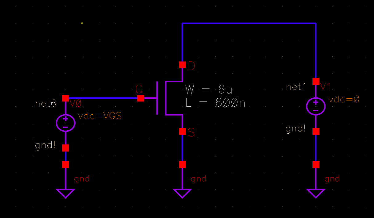
Figure 1 - NMOS Schematic
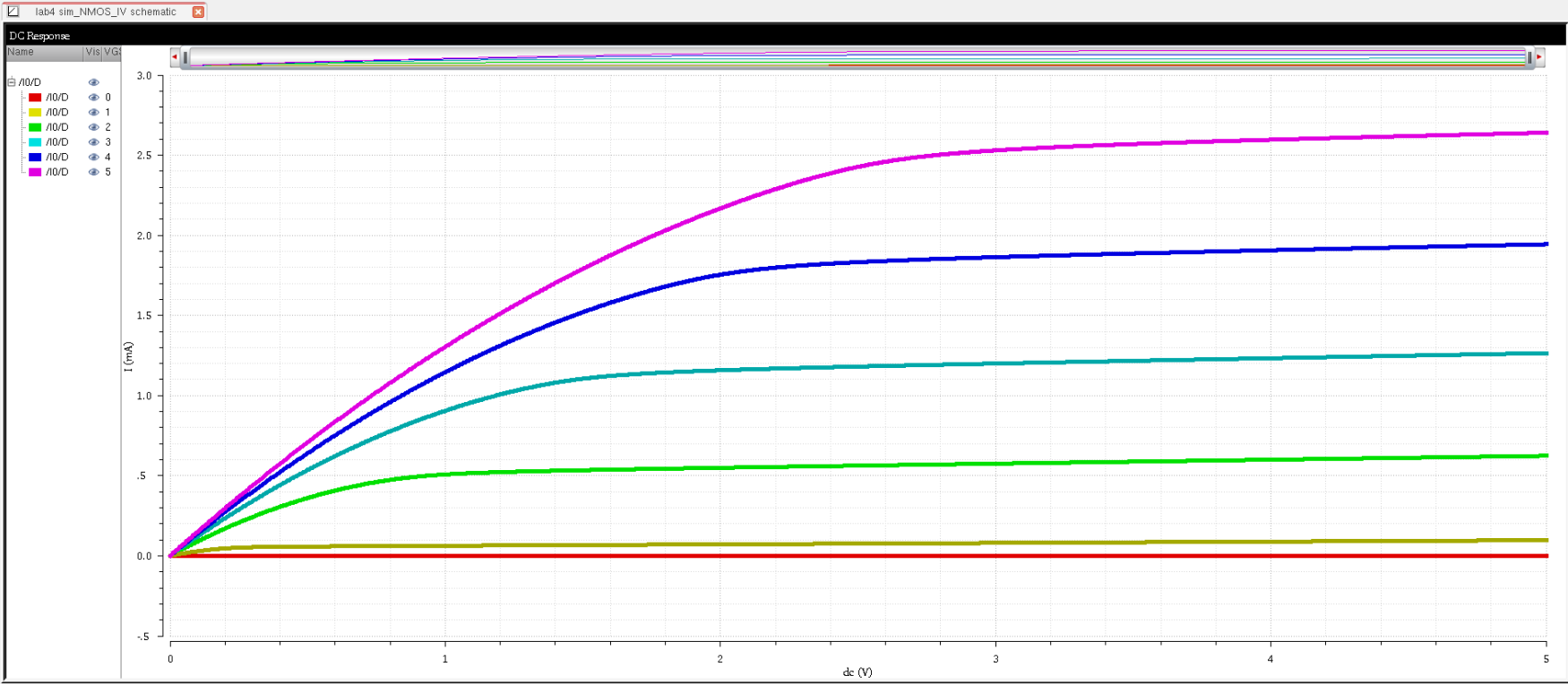
Figure 2 - NMOS IV Curves
The second schematic
will be another NMOS schematic with a varying VGS from 1V to 2V with a
1mV step whereas the VDS will be at a constant 100mV. The NMOS has a 6u/600n width-to-length ratio.
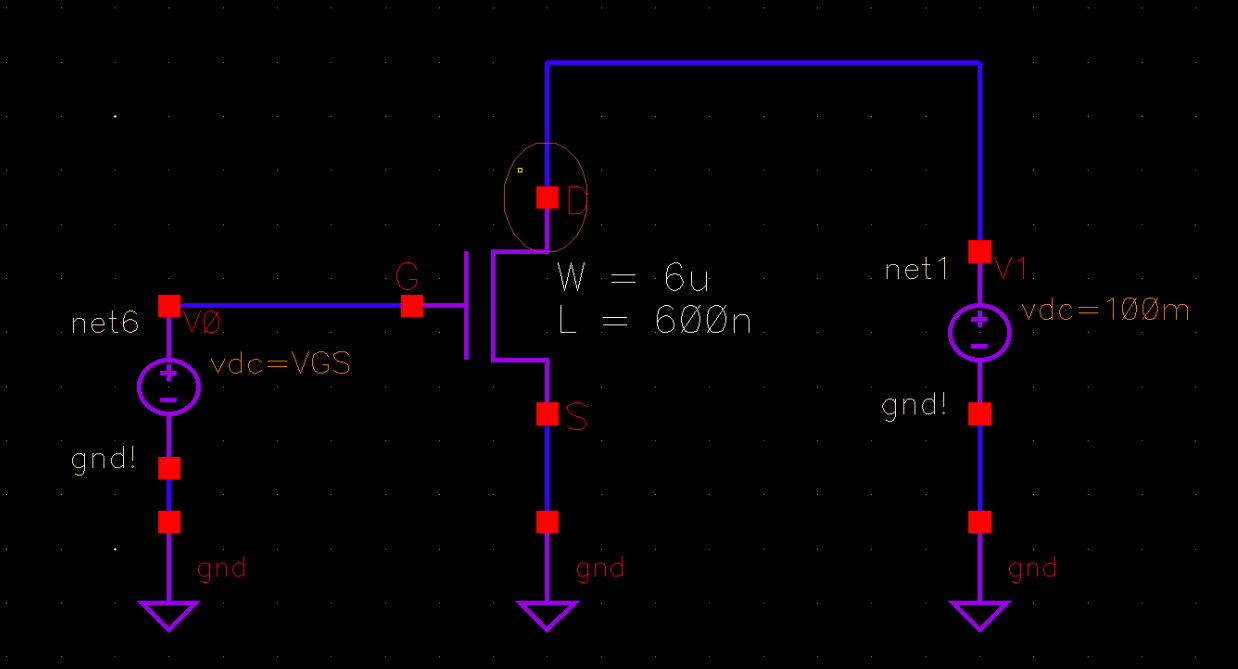
Figure 3 - NMOS Schematic with a VDS of 100mV
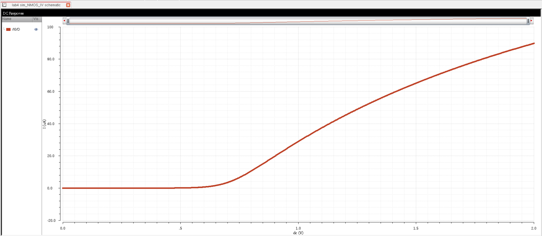
Figure 4 - NMOS IV Curve with Constant VDS of 100mV
The third schematic will be a PMOS with a varying VSG and VSD. The PMOS has a 12u/600n width-to-length ratio.
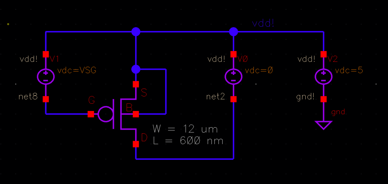
Figure 5 - PMOS Schematic
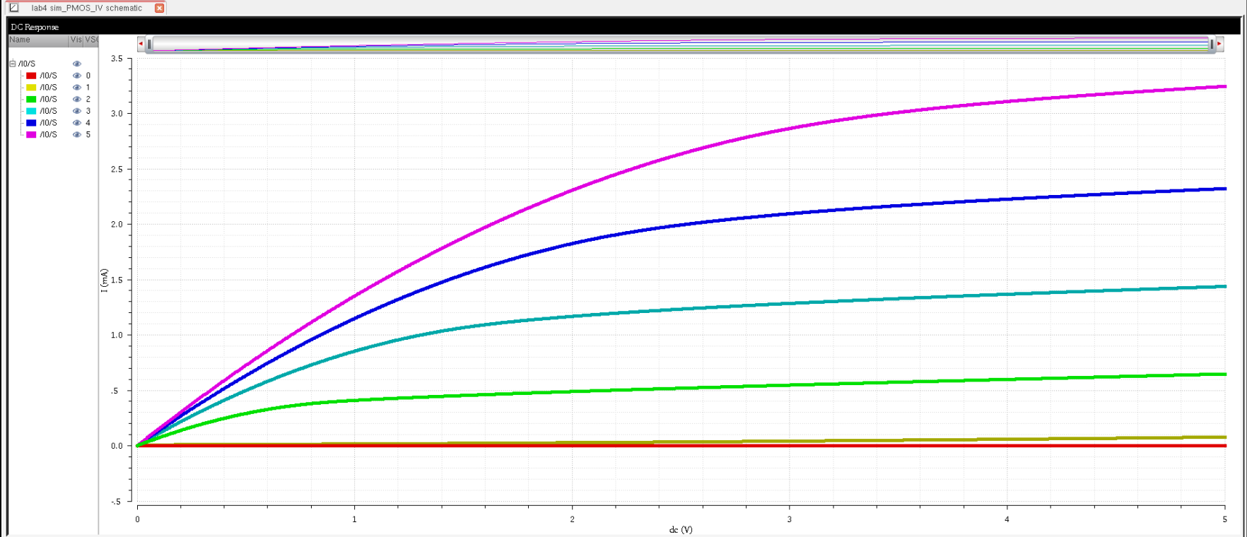
Figure 6 - PMOS IV Curves
The
fourth schemaatic will be another PMOS schematic with a varying VSG
from 0V to 2V with a 1mV step and a constant VSD of 100mV. The PMOS has
a 12u/600n width-to-length ratio.
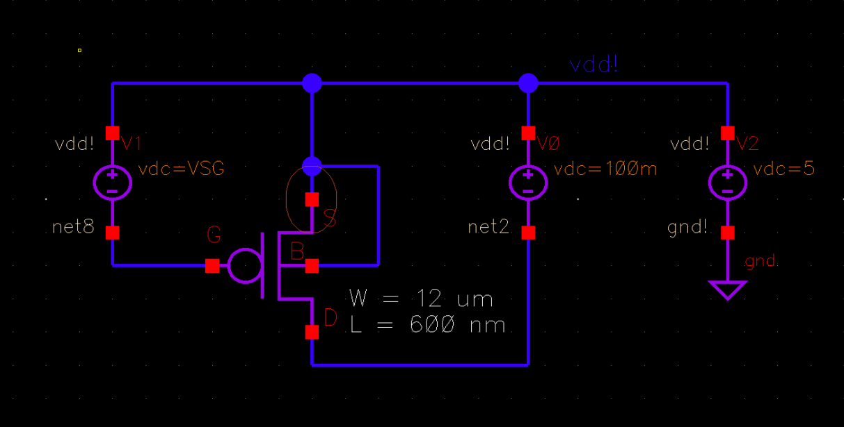
Figure 7 - PMOS Schematic With a 100mV Constant VSD
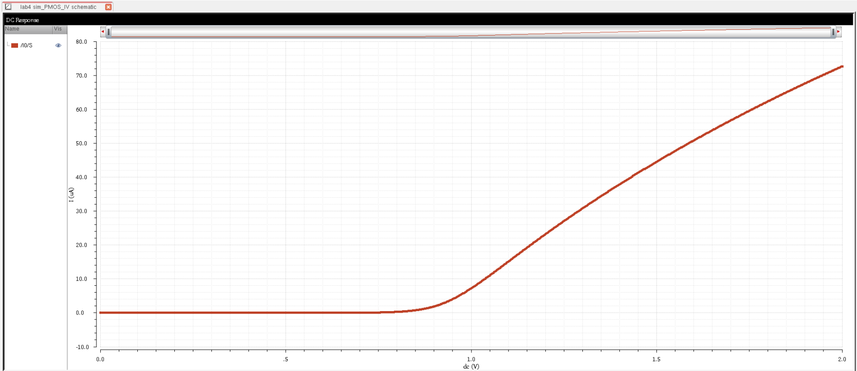
Figure 8 - PMOS IV Curve With Constant VSD
Part 2: NMOS Layout and Probe Pad
For
this part of the lab we will be laying out an NMOS and then connecting
the pins to a probe pad. The first thing we have to do is to create the
Probe Pad that we will be using for this NMOS and layout and the next
PMOS layout. The Probe Pad was created using a metal3 layer and glass
layer which is smaller in area than the metal 3 layer. The measurements
were based on the example given.
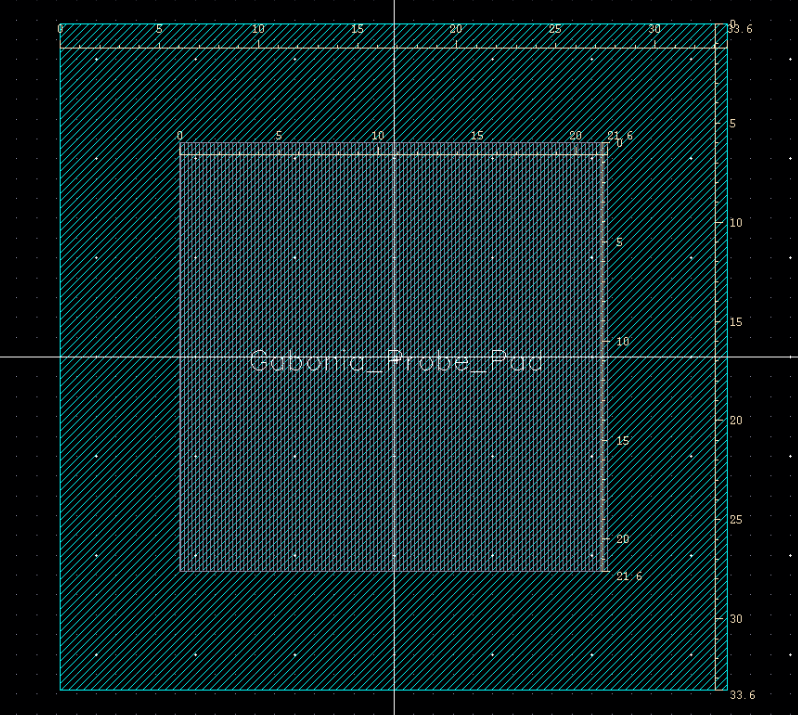
Figure 9 - Probe Pad Layout
After
creating the probe pad layout it is now time to create the schematic
and then a symbol which we will use with our NMOS schematic symbol.
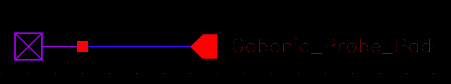
Figure 10 - Probe Pad Schematic
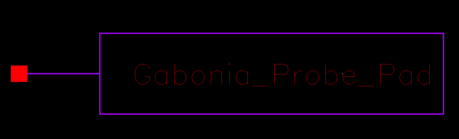
Figure 11 - Probe Pad Symbol
Now
that the Probe Pad is finished now we will implement the Probe Pad
Schematic Symbol into our NMOS Schematic which will be used for the LVS
after the layout is completed. This step just involves putting the
Probe Pad Symbol on all of the terminals on the NMOS.
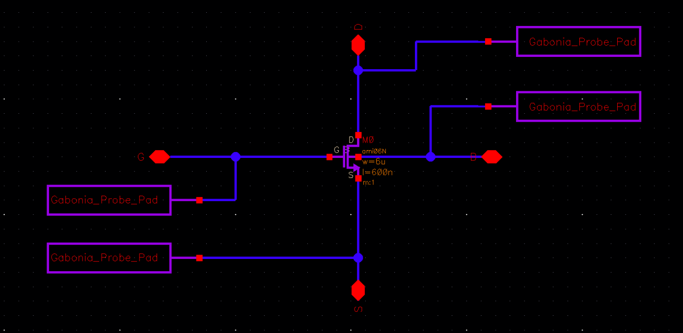
Figure 12 - Implementing Probe Pad Symbol into NMOS Schematic
Now
that the NMOS schematic is ready with the probe pads we can now set the
probe pads in the NMOS Layout. We will instantiate 4 Probe Pads and
then connect these probe pads to the 4 pins on the NMOS using metals
and vias.
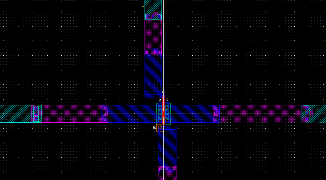
Figure 13 - Closer View of Layout of NMOS
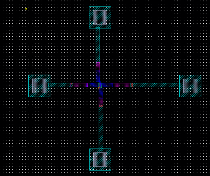
Figure 14 - NMOS Layout Zoom Out
Now
that the Layout of the NMOS is complete all that's left is to DRC the
layout, extract and then perform the LVS with the schematic we made and
make sure everything is good.
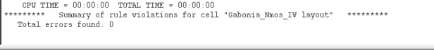
Figure 15 - NMOS Layout DRC
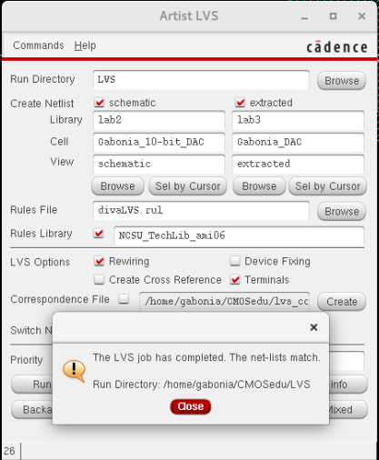
Figure 16 - NMOS LVS
Part 3: PMOS Layout and Probe Pad
For
this part of the lab we will be doing the same thing we did for the
NMOS but for a PMOS instead. Since the Probe Pad is already created we
can just implement it onto the PMOS schematic.
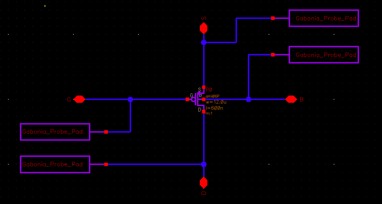
Figure 17 - PMOS Probe Pad Schematic
After the schematic is made we can implement the probe pad onto the layout and connect with metals and vias.
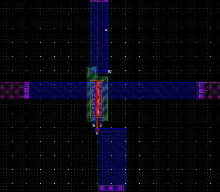
Figure 18 - PMOS Probe Pad Layout Close Look
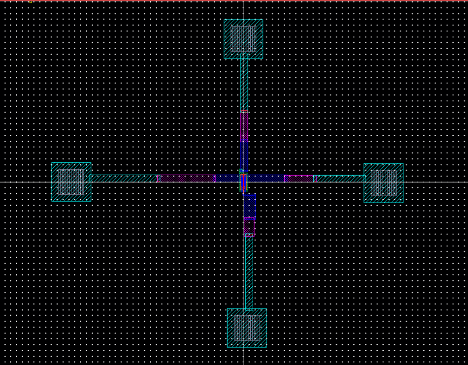
Figure 19 - PMOS Layout Zoomed Out
After the PMOS Layout is complete we can now do a DRC and LVS.
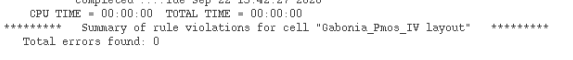
Figure 20 - PMOS DRC
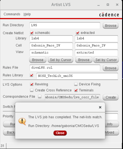
Figure 21 - PMOS LVS
lab4.zip
Return to EE421L