EE421L Project: High Speed Digital Receiver

Authored by Xianjie Cao

November 12, 2020


Project Description:

     Design, layout and simulate a digital receiver circuit that accepts a high-speed digital input signal, D and Di (a differential pair connected to the circuit from, for example, a twisted pair of wires such as an Ethernet cable). D and Di are complements so, for example, if D is 5V then Di is 0V then the output is 1. Another example, when D is 1V and Di is 2V then output is 0. The goal of the design is to see if we can get 250 Mbits/s with input voltage difference of 250mV that the circuit still outputs the correspondingly correct value in the C5 process.

    
Report Due Date:

    First half: schematic but no layout, and operation simulations. Due Nov. 18.

    Second half: a verified layout and documentation (in html). Due Nov. 25.


Schematic And Simulations:


Here is the NMOS version of the differential circuit that I'm going to use for the project, using 10/1 (6u/0.6u) MOSFETs.


http://cmosedu.com/jbaker/courses/ee421L/f20/students/caox2/Project/p1.png


http://cmosedu.com/jbaker/courses/ee421L/f20/students/caox2/Project/p2.png    http://cmosedu.com/jbaker/courses/ee421L/f20/students/caox2/Project/p3.png


The propagation low to high delay is around 300ps, and the high to low delay is around 230ps. Which are reasonable, so the circuit works with V_diff = 5V.


Note that, when the V_diff is small, for example, 250mV, then the circuit did not work quickly.


 http://cmosedu.com/jbaker/courses/ee421L/f20/students/caox2/Project/p4.png


So for low V_diff, we should use the PMOS version of the circuit.


Here is the PMOS version of the differential circuit.


http://cmosedu.com/jbaker/courses/ee421L/f20/students/caox2/Project/p5.png    http://cmosedu.com/jbaker/courses/ee421L/f20/students/caox2/Project/p6.png


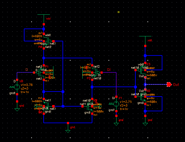
Note that when output approach to ground, there is an offset, to get rid of that offset, we could combine both the NMOS and PMOS version.


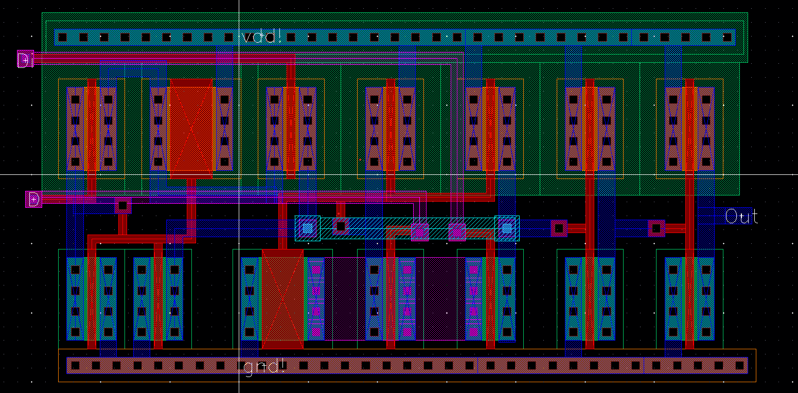
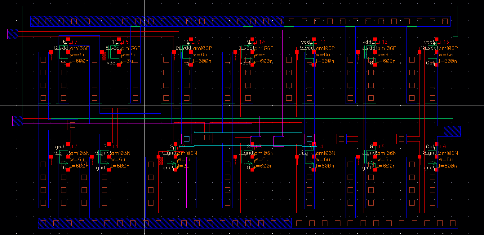
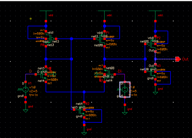
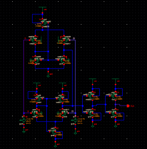
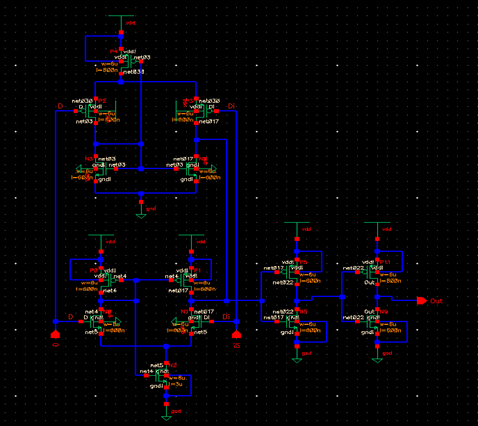
Here is the combined and the final version of the circuit.


http://cmosedu.com/jbaker/courses/ee421L/f20/students/caox2/Project/p7.png    http://cmosedu.com/jbaker/courses/ee421L/f20/students/caox2/Project/p8.png


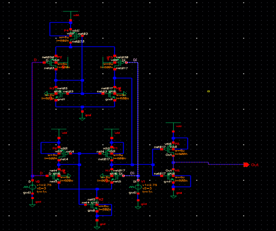
The output is not perfectly at Vdd or ground, so I added another inverter to the output, so it will square the output and to get the correct logic, that is, when D > Di, Out = 1, and 0 otherwise.


http://cmosedu.com/jbaker/courses/ee421L/f20/students/caox2/Project/p9.png    http://cmosedu.com/jbaker/courses/ee421L/f20/students/caox2/Project/p10.png


http://cmosedu.com/jbaker/courses/ee421L/f20/students/caox2/Project/p11.png    http://cmosedu.com/jbaker/courses/ee421L/f20/students/caox2/Project/p12.png


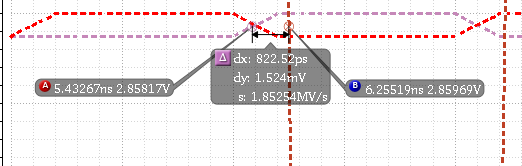
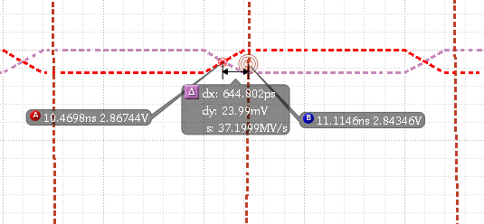
The propagation high to low delay is around 823 ps, and low to high is around 645 ps.


Since I was using the 6u/0.6 MOSFETs, whereas 0.6u is the minimal length for C5 process, which implies that this design would use more power. To reduce the power usage, in the meantime, for the circuit to still be fast, we can modify the size of the bottom NMOS and the top PMOS, in other words, we can use a longer L or shorter W to reduce the power, but in return, the circuit gets slower. 


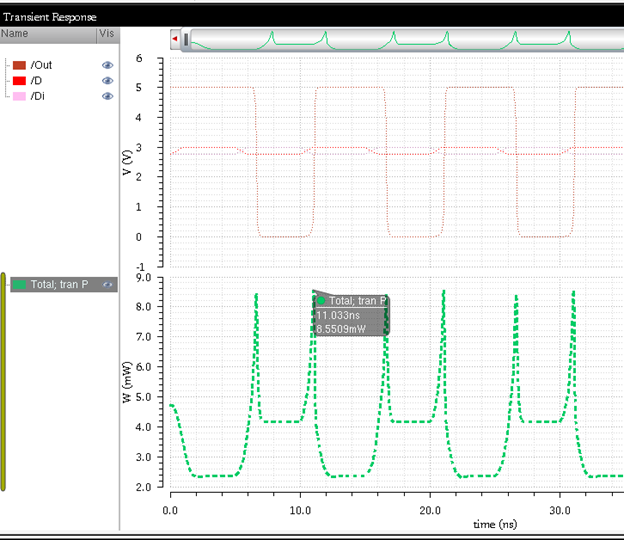
Power Dissipated can be calculated by:

P_avg = Vdd * I_avg = C_Tot * Vdd ^ 2 * f_clk. From this equation, we know that power is related to the input frequency and the total capacitance of the circuit, in other words, the size of the transistaors will also affect the power consumption.


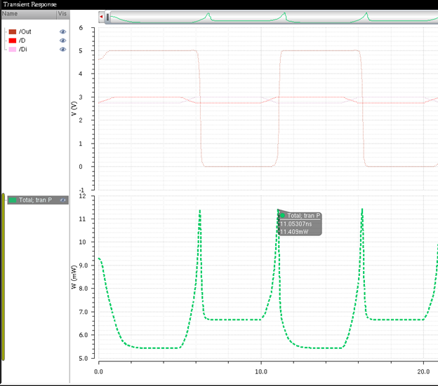
Here is the power for size of 6u/0.6u:


http://cmosedu.com/jbaker/courses/ee421L/f20/students/caox2/Project/p29.png


Size of 3u/3u:


http://cmosedu.com/jbaker/courses/ee421L/f20/students/caox2/Project/p13.png    http://cmosedu.com/jbaker/courses/ee421L/f20/students/caox2/Project/p14.png    http://cmosedu.com/jbaker/courses/ee421L/f20/students/caox2/Project/p15.png


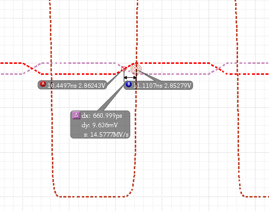
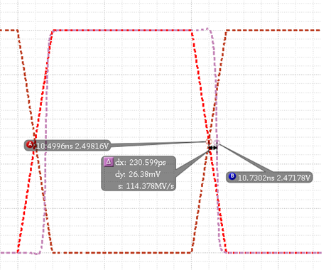
The propagation high to low delay is around 1.1 ns, and the low to high is around 661 ps. 


For my design, I wish to have delay less than the rise time and the fall time of the input, in this case, 1 ns, so I want it to be litter bit faster.
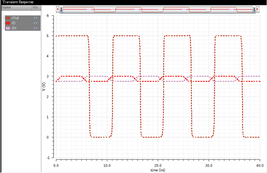
    

Size of 6u/3u:


http://cmosedu.com/jbaker/courses/ee421L/f20/students/caox2/Project/p16.png    http://cmosedu.com/jbaker/courses/ee421L/f20/students/caox2/Project/p17.png    http://cmosedu.com/jbaker/courses/ee421L/f20/students/caox2/Project/p18.png


Power for size of 6u/3u:


http://cmosedu.com/jbaker/courses/ee421L/f20/students/caox2/Project/p30.png


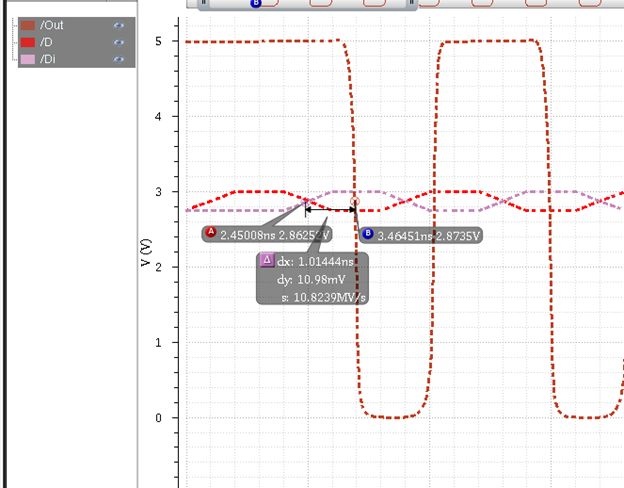
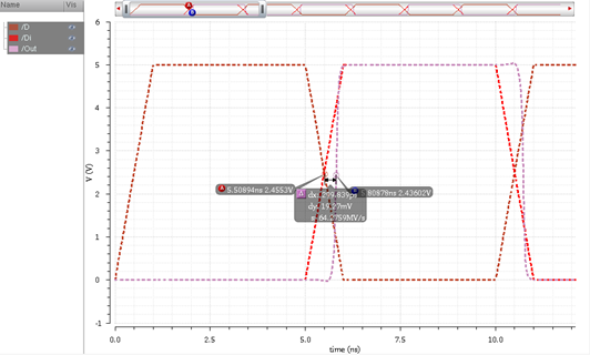
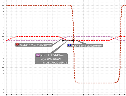
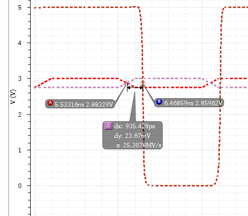
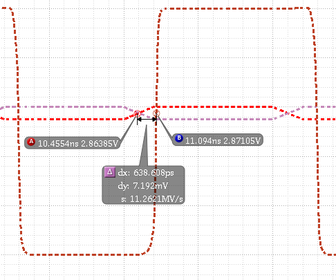
The propagation high to low delay is 935 ps, and thhe low to high is 639 ps. Both met my desired values, so this is going to be my final design.


http://cmosedu.com/jbaker/courses/ee421L/f20/students/caox2/Project/p19.png


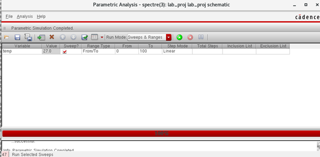
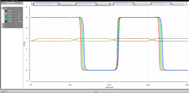
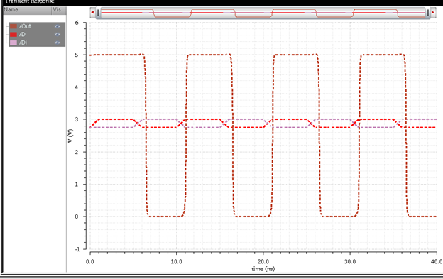
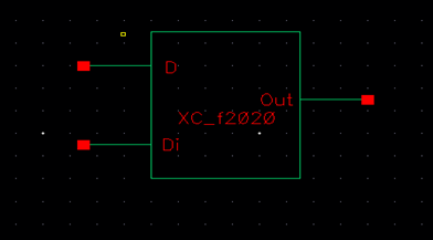
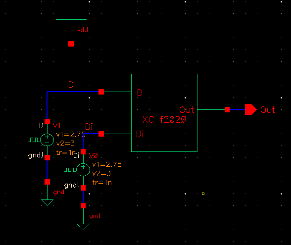
Next, I'm going to simulate my circuit to see what are the limatation of the circuit. Here is the symbol for the digital receiver and a circuit I'm going to use for simulation.

   
http://cmosedu.com/jbaker/courses/ee421L/f20/students/caox2/Project/p20.png    


http://cmosedu.com/jbaker/courses/ee421L/f20/students/caox2/Project/p21.png


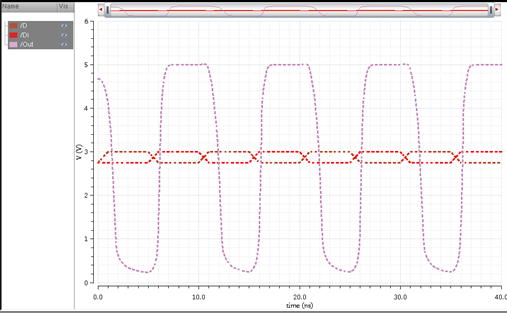
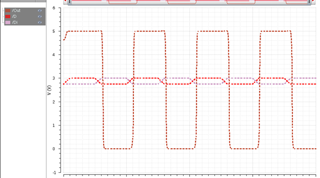
When D = 5V, Di = 0V, V_diff = 5V at 250Mbits/s:


http://cmosedu.com/jbaker/courses/ee421L/f20/students/caox2/Project/p22.png    


http://cmosedu.com/jbaker/courses/ee421L/f20/students/caox2/Project/p23.png


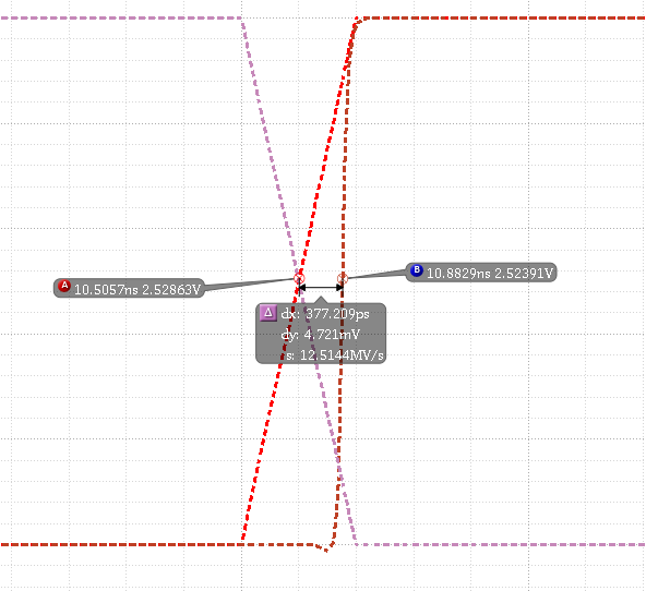
From the above simulation result, I know that my design works with high V_diff.


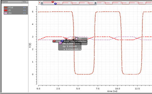
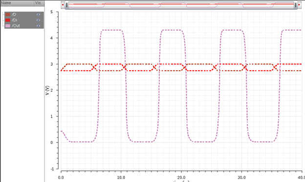
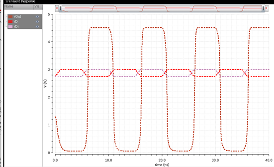
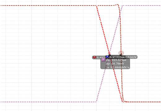
When D = 3V, Di = 2.9V, V_diff = 100mV at 250Mbits/s:


http://cmosedu.com/jbaker/courses/ee421L/f20/students/caox2/Project/p24.png 


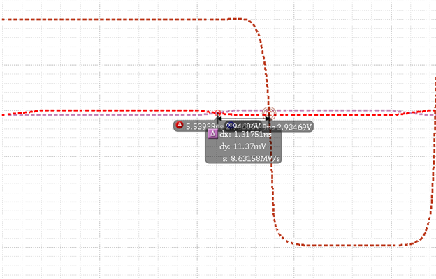
The propagation high to low delay is 1.31ns, and an offset is present too, so I might say that the performance of my design decline when V_diff < 100 mV.


When Bit width is 2 ns or 500Mbit/s:


http://cmosedu.com/jbaker/courses/ee421L/f20/students/caox2/Project/p25.png


The delay is around 1 ns, which is not too bad, now see if 1Gbits/s.


When Bit width is 1 ns or 1Gbits/s:


http://cmosedu.com/jbaker/courses/ee421L/f20/students/caox2/Project/p26.png


The delay is 1.01 ns, which is greater than the bit width, so I can conclude that my design works when < 1Gbits/s.


Hence for best performance, the limatations are V_diff > 100 mV and speed at < 1Gbits/s.


Lastly, I want to see if the temperature is going to affect my design, to do this, I ran the parametric analysis on Cadence, so the temperature changes from 0 Celsius to 100 Celsius.


http://cmosedu.com/jbaker/courses/ee421L/f20/students/caox2/Project/p27.png    


http://cmosedu.com/jbaker/courses/ee421L/f20/students/caox2/Project/p28.png


As seen above, When the temperatue increases, we will get a longer delay, that's because the drain current of a MOSFET degrades when the temperature is increased.

End of the First Half. 

Second Half: Layout of the Digital Receiver


Now we've verified that the circuit is working, we can start to layout the circuit.


Layout View:


http://cmosedu.com/jbaker/courses/ee421L/f20/students/caox2/Project/p31.png


The Extracted View:


http://cmosedu.com/jbaker/courses/ee421L/f20/students/caox2/Project/p32.png


DRC Verification:


http://cmosedu.com/jbaker/courses/ee421L/f20/students/caox2/Project/p33.png


LVS Matched:


http://cmosedu.com/jbaker/courses/ee421L/f20/students/caox2/Project/p34.png


The end of the second half. 


lab_proj.zip    


Return to EE421L Labs