Lab 7 - EE 421L Fall 2020
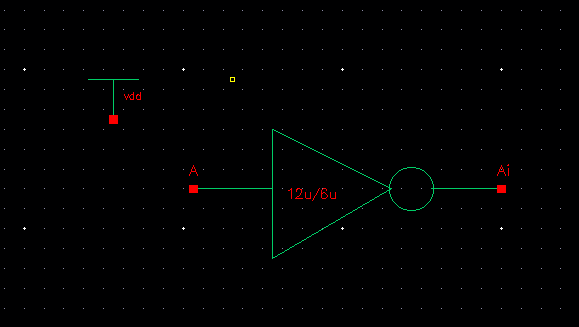
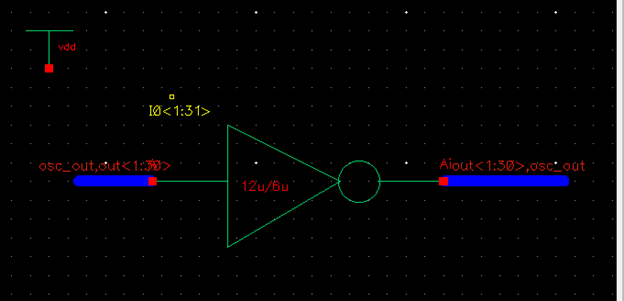
The Schematic of the inverter is as seen below, and we will use 31 of them.
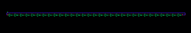
So the schematic for the ring oscillator is as such:
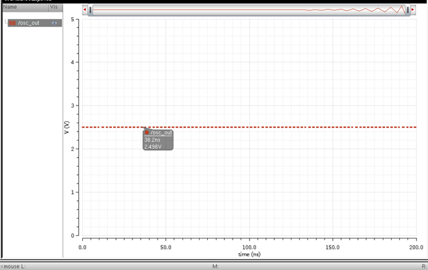
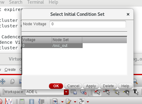
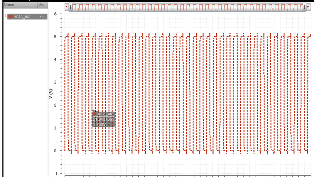
That's because we did not have a initial conditions, with the initial condition, the output is as following:
We can also optimize our schematic by using wide wire, the following circuit is identical as the previous one.
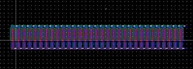
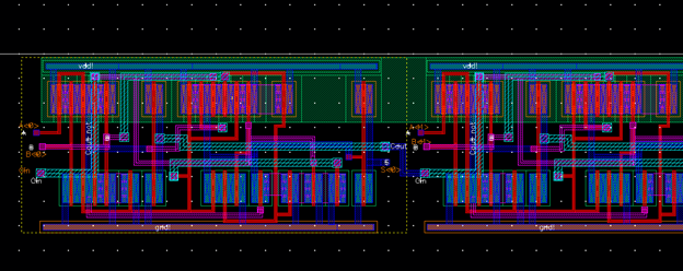
The layout of the ring oscillator with evidence of passing DRC check.
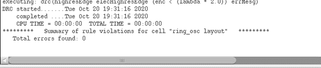
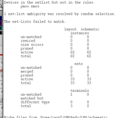
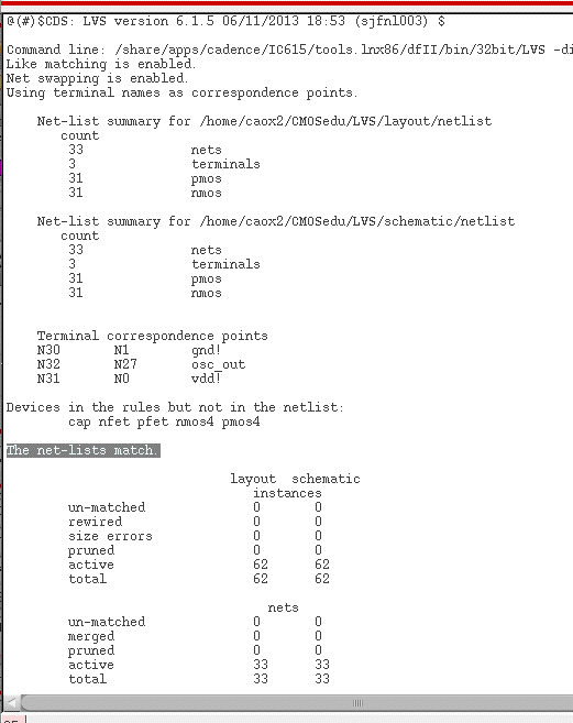
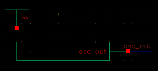
However, the LVS did not match. The reason is that we have osc_out pin in our layout but not in our schematic.
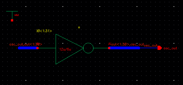
So let's add a pin called osc_out and as an output.
Then the LVS matches.
Now moving to create a symbol for the ring oscillator.
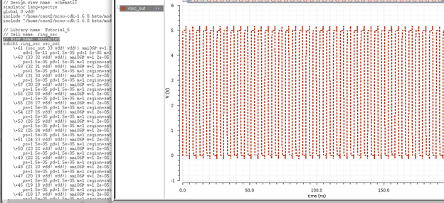
Lastly, we'll simulate the extracted view, it is as following:
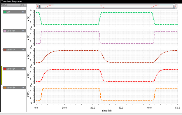
2) Circuit used to simulate thhe function of the 4-bit inverter.
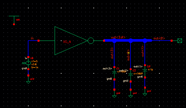
Note that, output<1> to output <3> were all connected to a capacitive load, 100ft, 500ft and 1p ft, so the output was smoothing out.
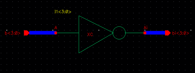
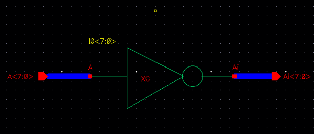
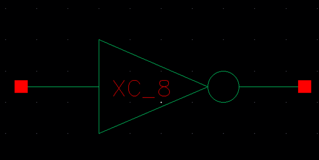
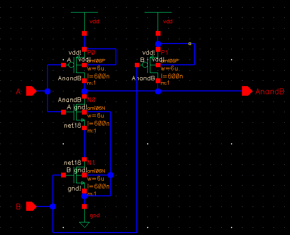
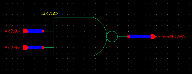
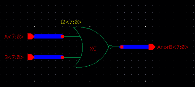
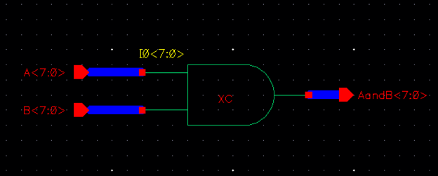
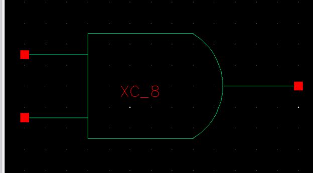
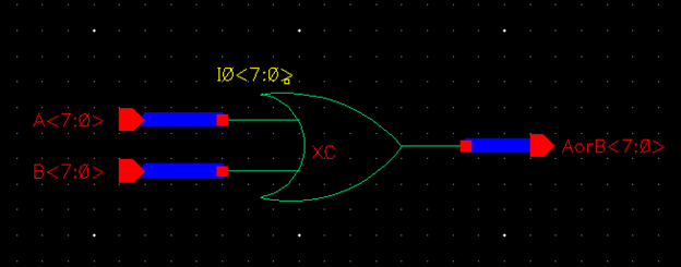
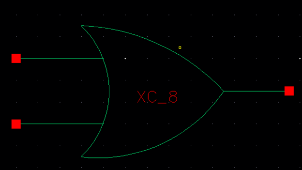
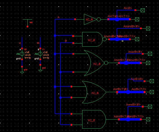
3) The schematic of the gate (1-bit), then followed by the 8-bit schematic and its symbol.
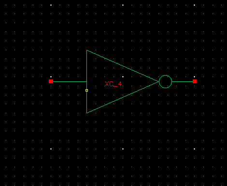
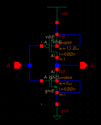
Inverter:
NAND gate:
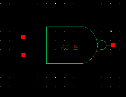
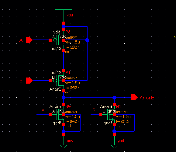
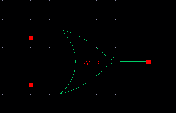
NOR gate:
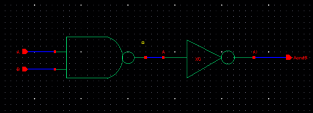
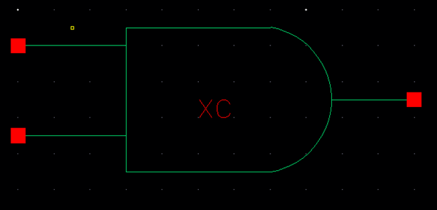
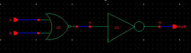
AND gate:
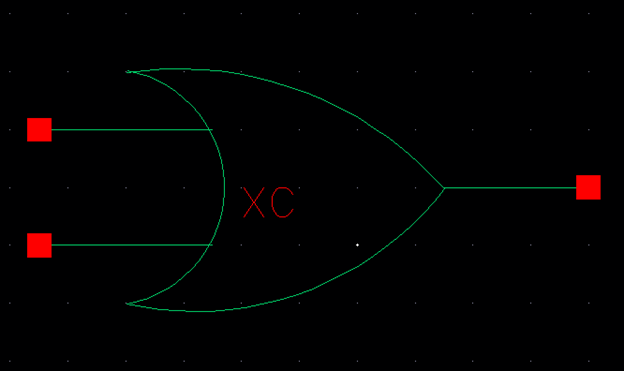
OR gate:
4) The symbols have been created, it's time to simulate them to make sure they all function correctly.
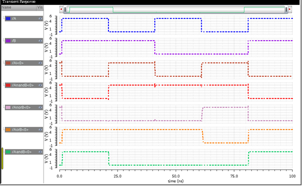
from the simulation result, it's clear that all gates work correctly.
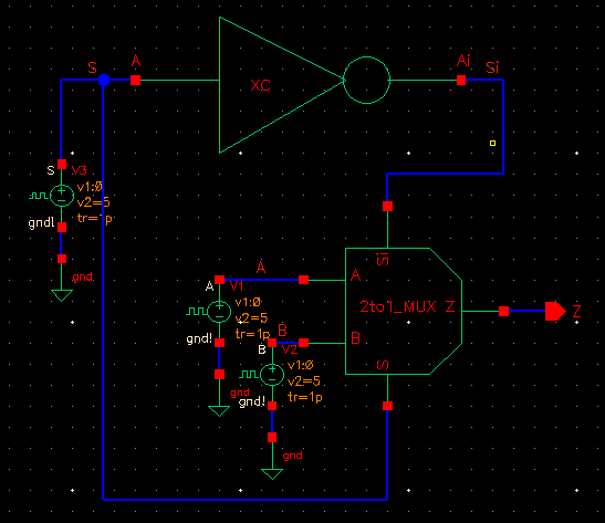
5) 2-to-1 MUX or 1-to-2 DEMUX
This is the schematic for 2-to-1 MUX, note that there is only one output (Z), other pins were created as inputs.
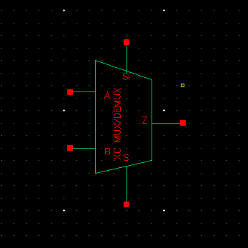
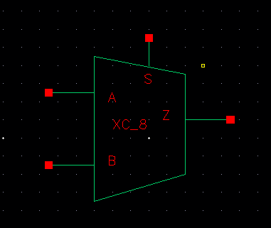
The symbol of the MUX and the circuit for verifying its functionality :
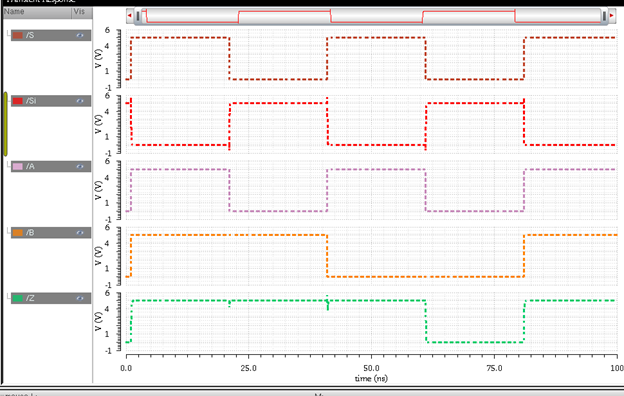
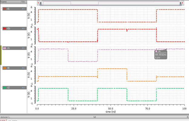
When S goes HIGH, input A propagates through.
When Si goes HIGH, input B propagates through.
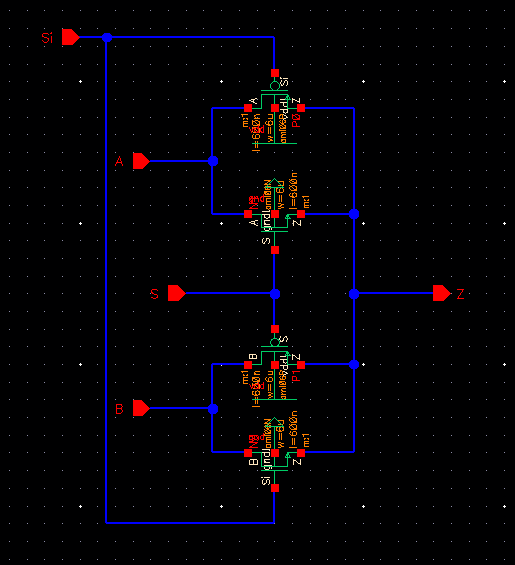
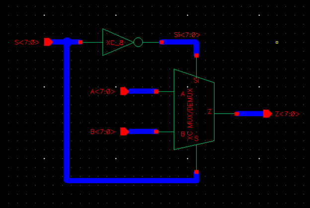
We now combine the MUX to make a component that acts as both MUX and DEMUX.
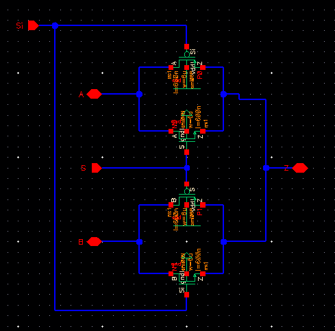
Note that PIN A, B and Z were created as inputoutput type, so they can be either input or output..
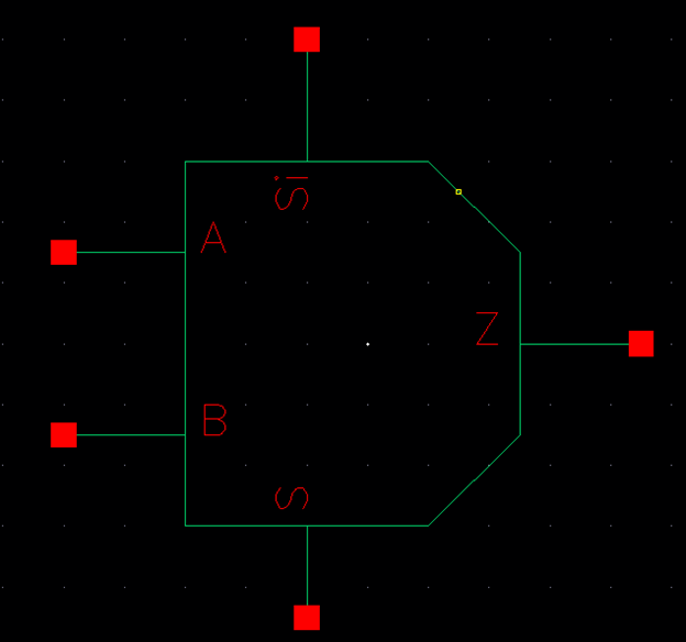
The symbol and the simulation result of the DEMUX/MUX:
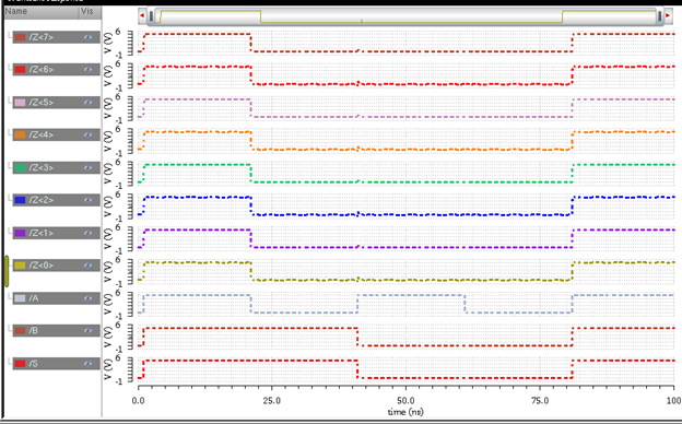
8-bit schematic and its symbol:
The simulation result of the 8-bit MUX/DEMUX:
When S goes HIGH, input A propagates through.
When S goes LOW, input B propagtes through.
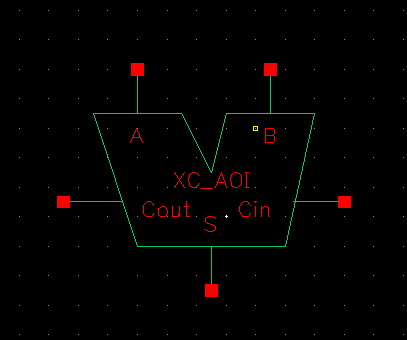
6) The AOI full-adder
The schematic and its symbol:
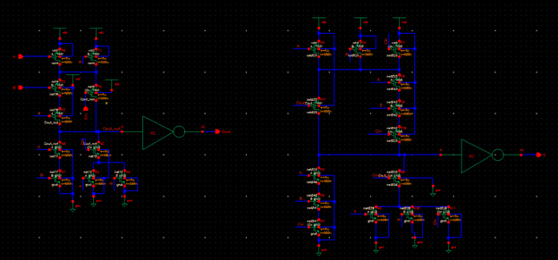
The schematic and symbol of the 8-bit AOI full-adder:
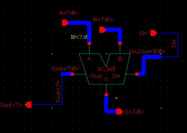
Circuit used to verify the adder's functionality.
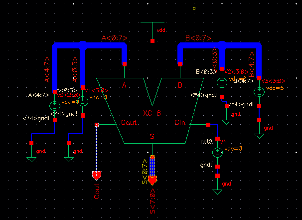
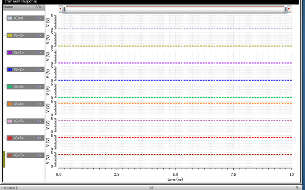
A = 00000000 (decimal 0), B = 11110000 (decimal 240), Sum = 11110000 (decimal 240).
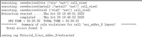
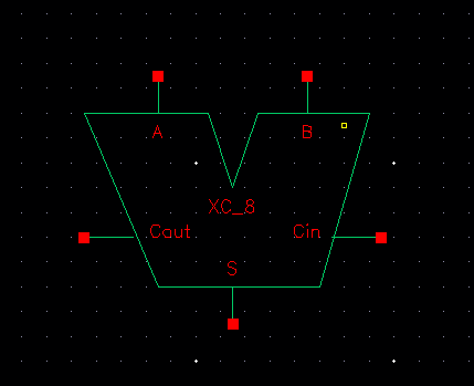
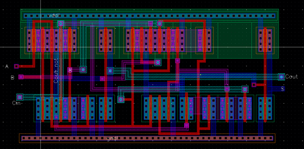
7) Layout of the Full-Adder
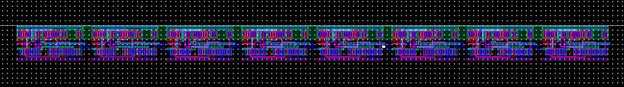
Layout of the 1-bit full adder:
Extracted view:
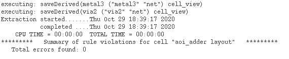
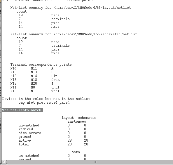
With no DRC errors and it passes LVS test.
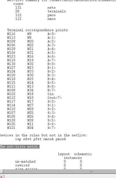
The Layout of the 8-bit full adder:
Extracted view:
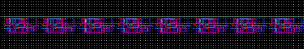
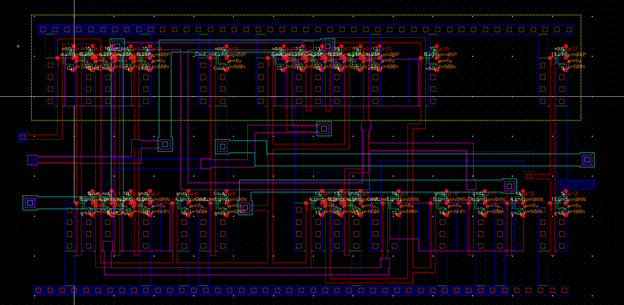
Zoom in view of the Layout:
With no DRC errors and it passes the LVS test.