Lab 6 - EE 421L Fall 2020
Authored
by Xianjie Cao
6 October, 2020
Pre-lab:
Our pre-lab work includes design, layout and simulation of a CMOS NAND gate.
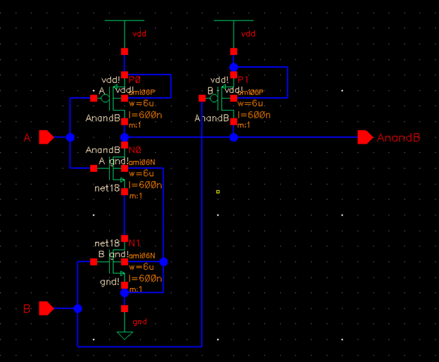
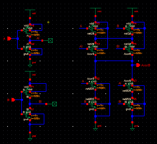
The schematic of the NAND gate is as following, it's using two 6u/0.6u PMOSs and two 6u/0.6u NMOSs.
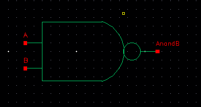
Symbol of the NAND gate:
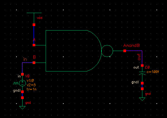
To
testify whether the NAND gate is working properly, we'll make a circuit
as below then simulate the operation of the NAND gate.
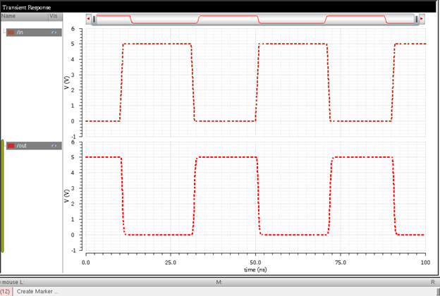
Simulation result:
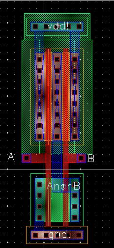
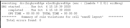
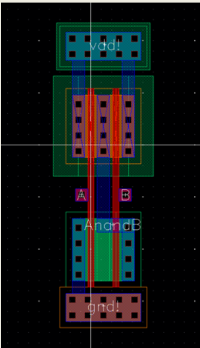
We'll then layout the NAND gate. (showing that it has passed the DRC and LVS)
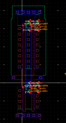
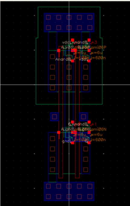
Extracted view of the layout:
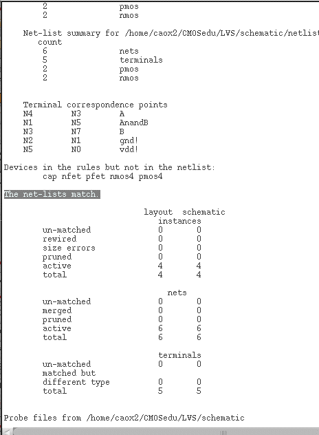
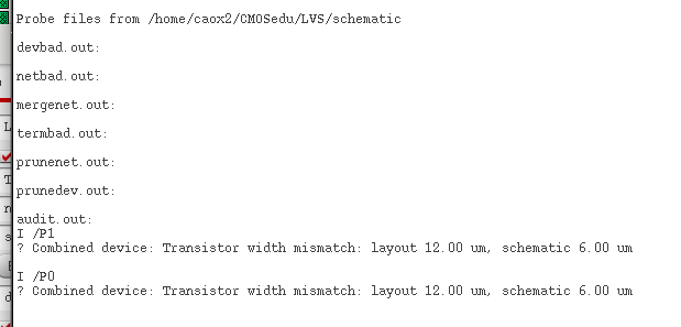
Since
the size of the PMOS devices in shcematic is differ from the PMOS in
the layout. We can enable the FET parameters comparison, then re-run
the LVS.
Lab
description:
Draft the schematics and layouts for a 2-input NAND gate and a
2-input XOR gate using 6u/0.6u MOSFETs transistors. Create symbols for
both of them, and then verify their functionalities. Lastly,
built a full adder using the NAND and XOR gates, both the layout and
schematic, make sure it passes DRC and LVS.
Lab procedure:
1) Schhematic and symbol for the 6u/0.6u NAND gate.
2) Layout of the NAND gate with evidences showing that it passes DRC and LVS.
3) NAND gate circuit for simulation.
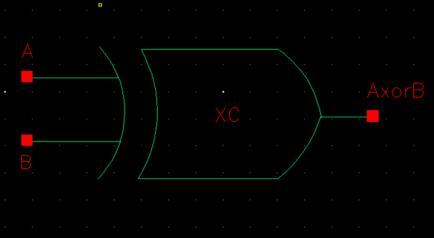
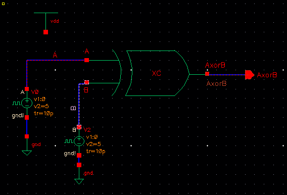
4) XOR gate schematic and symbol.
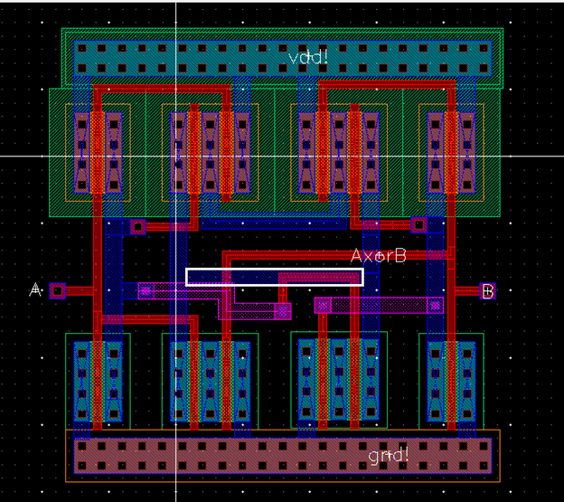
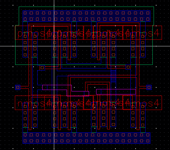
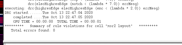
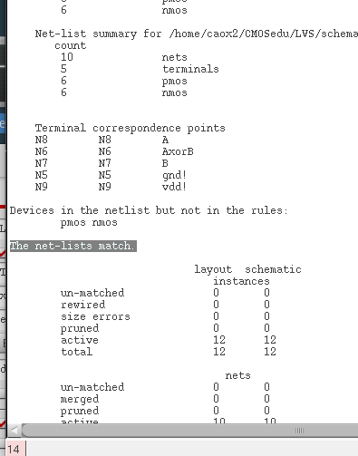
5) The Layout of the XOR gate, with evidences showing that it passes the DRC and matches the LVS.
6) XOR gate circuit for simulation.
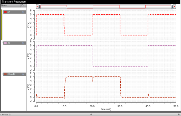
Because
of the rise and fall time of the both A and B inputs, it causes
Glitches in the output, during that period of the rising and falling
input, those gates are neither on, nor off.
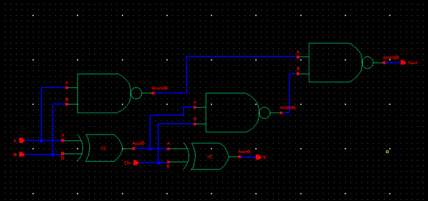
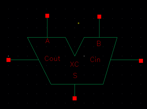
7) Full Adder schematic and symbol.
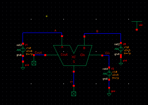
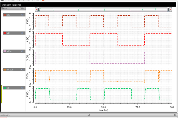
8) Full Adder circuit for simulation, showing all the 8 possible cases.
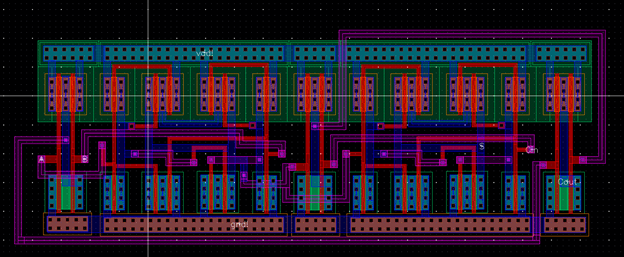
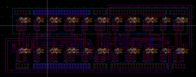
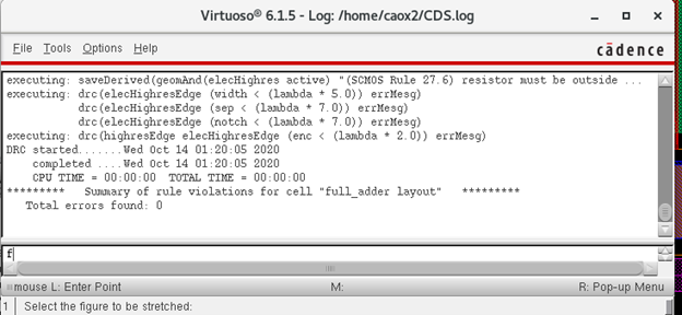
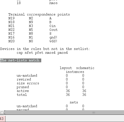
9) The layout of the Full Adder with evidences that it passes DRC and matches the LVS.
For back-ups:
Zipped
the library folder and the folder that has all the collected images to
the desktop, then upload them onto my personal github repository for
backups.

Return to EE421L Labs